


")

Reception of television programs through satellite repeaters has become today the sign of the day. Increases the number of satellites in the geostationary orbit and the number programs on each of them. To purchase a receiving system NTV in the store is not has become a problem, and Yes the prices are reduced. Buying equipment factory manufacturing, many hams are experimenting with it. We also have enthusiasts who produce such equipment themselves. Here we publish the description of the simple devices for the optimal settings of all components receiving system NTV.
Reception of television programs through satellite repeaters interested in all a larger circle of readers. With the launching into geostationary orbit satellites systems direct television (NTV), for example. "Gals" and "Ноt Bird", this technique became available to many people in our country (low cost equipment, small the dimensions of the antenna). At the same time for ham radio interest and other satellites, from which the signal is much weaker, and to obtain satisfactory quality of reception is necessary to apply large antenna sizes.
One of the problems that must be addressed in these experiments, - debug antenna system and adjusts it to the desired satellite peak. For systems NTV, using relatively powerful transmitting devices, this problem solved easy as possible the use of antennas with a small diameter parabolic mirror. Such antenna beam width is a few degrees, so small inaccuracies when you hover perfectly acceptable and not even a very strong impact on the final result. More the case when an antenna of large size and weak signals are accepted. This requires very careful and careful tweaking.
Significantly reduce the complexity of this process, to simplify and make it visual visual will help described below, a combined unit, in which combination with the oscilloscope can be used as a panoramic indicator spectrum frequency range 0,8…HTC or indicator frequency response in that range, and without oscilloscope - as an indicator of the signal level on any part or all range. With the help of the device it is possible for the noise to quickly assess the serviceability Converter, to test the tuner, if necessary (if, for example, home-made or works for a long time) to adjust the AFR and the range of adjustment. The device will help you to quickly tune to satellite signals and to adjust the antenna system for maximum signal, to clarify the placement of the Converter (irradiator), to adjust its polarization, etc. the Main convenience is that the results of manipulations affect immediately the oscilloscope screen or a dial indicator.
Diagram of the device and its design is quite simple and easy to manufacture radio Amateurs of average skill. The structural scheme is shown in Fig.1. In it includes current-controlled sweep generator (G1) -generator ultra high frequency tuning range of 0,8…2 GHz buffer amplifier And 1, the output of which the signal at the scale of 1; 1 to appear on the output "sweep 1 :1", and through a resistive attenuator A2 - exit "sweep 1:10". To manage generator designed shaper triangular voltage (G2) and the voltage-to - current - (U1). Install the upper and lower frequencies swing band performed independently from each other using variables resistors, which is convenient when operating. Amplifier AL is used for the signal the sweep of the oscilloscope. Eat these nodes from the network power supply unit (U2).
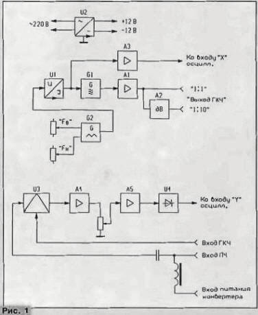
These elements together with the detector head is provided panoramic mode display frequency response. For this purpose, the input "Y" of the oscilloscope the signal from the output the detector head, and the input "X" is the sweep signal from the output of amplifier AZ. For implementation of spectrum analyzer mode the device has a mixer (U3), which with the release of "sweep" through the entrance of the "sweep" appears the signal generator, and through enter "FC" is the output signal of the UHF Converter. The output signal of the mixer amplified by video amplifiers (A4 and A5), detected by the amplitude detector (U4), the output of which a signal can be sent either to the input "Y" of the oscilloscope, either on the dial gauge. The device has slots for power Converter. The spectrum analyzer works with so-called "zero-if", allowed in case of satisfactory quality to simplify the construction of the device. The device is made of four main components: a high-frequency block, the shaper control voltage and current, amplifier and block power. Each of the blocks assembled on a separate printed circuit Board. This allowed to produce and regulate them separately from each other, and only then to install in the housing.
The high frequency circuit block shown in Fig.2. Transistors VT1 and VТ2 made the microwave generator, the frequency of oscillation can be controlled using current and VТЗ buffer amplifier. The signals output from the amplifier comes on nests ХS1 "1:1" and ХS2 "1:10". Further details of these sites were previously described in [1].
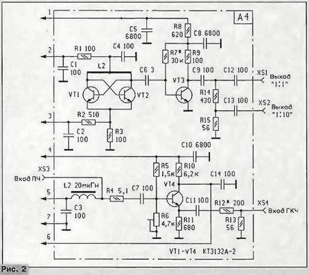
Transistor VT4 assembled the mixer signal is in the analyzer mode spectrum. At its base via socket XS3 receives the signal from the microwave Converter, and the emitter via socket XS4 - signal generator. For this nest ХS1 and ХS4 connect the coaxial cable. The difference signal is removed from the manifold transistor VT4 and then goes to the input of the amplifier, the capacitor C14 when this suppresses high-frequency components of the difference signal. Food microwave Converter is carried out via a low pass filter L2C3.
Diagram of the shaper control voltage and current is shown in Fig.3. On chips DА1 - DAZ DD1 and assembled shaper triangular voltage, which works in conjunction with a controlled current regulator on the chip and DА4 transistor VT5, DА5 assembled signal amplifier of the oscilloscope sweep. The amplitude of this voltage can be adjusted by the variable resistor R27. Resistors R17 and R20 are used to set the lower and upper frequency swing band frequency of the microwave generator. This node is executed according to the scheme [2] and therefore here not described in detail.
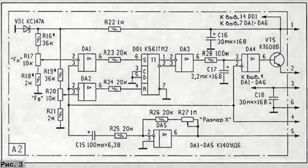
Diagram of the amplifier shown in Fig.4. He is two; each of them performed at a high speed op amp. The gain of each stage is 38 to 40 dB, which provides the required sensitivity of the analyzer spectrum. The adjustable gain is a variable resistor R32.
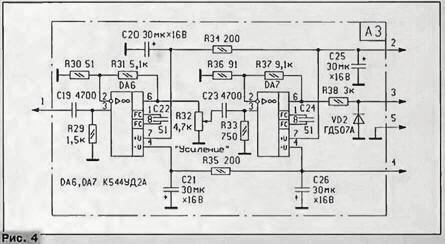
At the entrance of each cascade air filters high frequencies C19 R29 and C23 R33, which are designed to reduce the influence of low-frequency interference and noise. Special high pass filter in the amplifier no. it is the role of choose the OS, which provide end-to-end bandwidth of the analyzer in several hundred kilohertz. The output of the second cascade installed detector diode VD2 which cuts off the negative half of the signal, and the input "Y" or dial indicator receives the positive half of the AC voltage signal.
The power supply is built according to the traditional scheme (Fig.5) and contains a step-down the power transformer T1, full-wave rectifier diode matrix and VDZ smoothing capacitors C and C. Voltage stabilizers is made by well-known scheme and do not require comments.
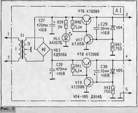
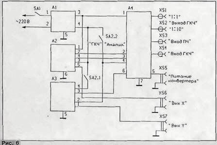
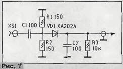
Diagram of Board-to-Board connections shown in Fig.6. Turn on the unit by switch SА1, and the operation mode switch SА2. These switches and variable resistors R17, R20, R27, R32 come on the front panel of the device. As in Fig. 7 shows a diagram of the detector head. It the main purpose is the detection of the microwave signal.
As mentioned above, the device can be used as an indicator of the frequency response analyzer spectrum or the signal strength indicator. In the first case, the device works in conjunction with the oscilloscope, the input "X". At its input a signal from the output ХS6 ("O. X") of the device and install scan the whole screen. On the oscilloscope will appear glowing horizontal line, called "zero", place it on the bottom line of the screen mesh.
The input "Y" of oscillograph connect the output of the detector head and the entrance to output Jack ХS1 ("sweep Output 1:1"). This will appear on the screen inclined or somewhat curved line, whose height relative to the zero line will be proportional to the signal level of the microwave generator, this line will provide a reference. Then a detector head is connected to the output or checkpoint investigated device, and a signal from nests ХS1 ("sweep Output" 1;1 or 1:10) is fed to the input device. Comparing the position of the reference line and the line, resulting in this case, it is possible to judge that runs the microwave signal through this device or not, increases in one or attenuated signal, and what is its frequency response. So it is possible to check the serviceability of tuners, amplifiers, signal splitters, etc. The range in which these parameters are investigated, is set by resistors R17 and R20 (block shaper, Fig.7), and can range from a few tens MHz to the full range. In this mode, the mixer and the amplifier do not work, because meals are not served.
In spectrum analyzer mode, all device nodes, sockets ХS1 иХS4 connect the cable, and the socket ХS3 ("Input FD") connect the output of the microwave Converter. At the same time on the oscilloscope screen should be a blurry line, so called "noise track". After supplying the supply voltage to the Converter (Jack ХS5) the noise level should increase its amplitude can to adjust the resistor R32 (block amplifier).
When you move the antenna in space at the time settings on the satellite on the screen the oscilloscope will appear noise-like bursts of signal at the place of the sweep, which corresponds to the frequency of this signal. By using variable resistors adjust the range of the oscillation frequency, this signal can "expand" on the whole screen. You can then configure the antenna system, to change the polarization and corners settings to obtain the maximum amplitude of the received signal. This setting allows you to squeeze out of the system possible. Distribution signals in the range of frequencies and their relative power determine what the satellite tuned antenna. If in this mode the Output Y" of the device to connect pointer indicator, for example, a microammeter with a current total deviation 100 μa. the deflection can judge about the level change the received signal, and therefore, it will be convenient to configure the antenna system on the signal maximum.
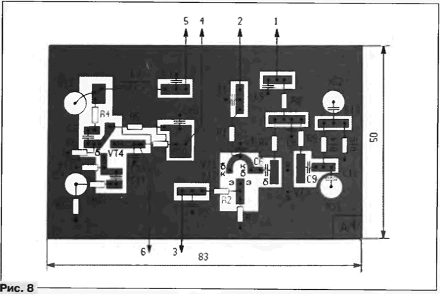
A sketch of the PCB high-frequency part is shown in Fig. 8. It is made of bilateral folgero-finished fiberglass. The conductors are located on one her side, and the other left metallized (it serves as a screen) and connected in circuit with a common power bus of the first party. The fee is placed on the side wall of the casing and attached thereto four microwave output jacks. This ensures that the minimum distance between the high frequency connectors and components on the Board.
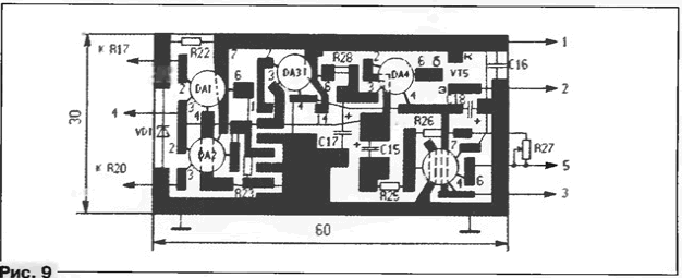
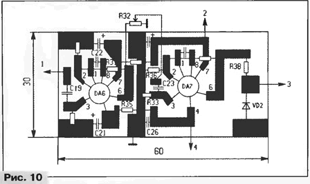
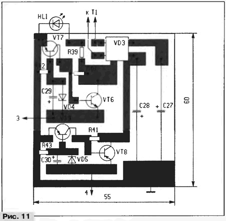
Sketches printed circuit boards shaper, amplifier and power supply are listed respectively in Fig. 9, 10 and 11. For their production you can use sided glass material. These boards are then placed on the bottom of the hull of the device on a metal plate (or of one-sided glass fiberglass, Micarta), which serves as the common wire and which connected to a common power bus of all boards.
The device is permissible to apply elements of the following types: chip DA1 - DA5 - CUT, CUT, DA6.DA7 - KUA, KUB, DD1 - KTM or other, contains an RS flip flop. Transistors VT1 - VT4 - CTA - 2, CTB - 2, CTV - 2, CHA - 2, CTB - 2, CTV - 2; VT5 - CTA, CTB, with CT alphabetic indices from A to G, KT(A - E); VT6 - CT(A - G), CTA, CTB, CTA, CTB; VT7 - KT315(A - I), KT(A - B), KT3102(A - E); VT8 - CT(A - M), KT(A - M); VT9 - CT(A - M), KT(A - M), KT(A - IN),KT361(A - E).
Diodes VD1 - XA; VD2 - D9 with any letter index, D18, D20, D, DA, DB, DA, DB; bridge VD3 will replace the four diodes types KD102B CDB, KD105B, CDA, KDA, KDA; VD4, VD5 - DG, XI, XZ, XA; CBE-todiode HL1 - AL307 with alphabetic indices from A to G or IL (A - D) oxide K50-6, C50 - 24, K53 - 1; as C1 - C14 desirable to use caseless K10 - 42, K10 - 17 or similar, in their absence (as an extreme case) will fit km, KD with the least possible length of the pins; the rest KLS, KD, KT, KM.
Variable resistors - CSP, SP4, SP any modification, trim (R6) - SDR - 19, other - MLT, S2-33. In the high-frequency device design it is desirable to use resistors C2 - 10.
The inductor L2 - DM - 0.1 inductance 20 - 100 µh. Step-down transformer - any small, having two secondary winding voltage of 12…15 In at currents up to 70 mA.
In the detector head should be used the microwave detector diodes, capacitors, in the high-frequency part of the device, and resistors C2 - 10.
Instrument setup start with the adjustment of individual circuit boards of the device. Block power setting, is usually not needed. You only have to check it out efficiency - output voltage must be between 11…13 V. If it is planned to power the Converter from the same power supply, you need a few umos-thread it - the transformer must provide current up to 200 mA; stabilizer will work the same, only the transistor VT6, if he starts to warm up much, might have to put on a small heatsink.
Driver control voltages pre-check as follows. To the Board connect the resistors R16 - R21, which are placed on the front panel. The findings of boards 2 and 4 temporarily close, and between them and the common wire install additional resistor of 200 Ohms, then served of the supply voltage. Upon rotation of the resistors R17 and R20 extra the resistor with an oscilloscope check the vibrations of triangular shape, the maximum the amplitude should be at least 1…1.5 V.
Then check the charge amplifier - it should not be instituted in any the position of the slider of the resistor RЗ2. If this happens, you may have parallel to the capacitor C20. C21, C25, C26 to install ceramic capacitors 0,047 - 0.1 µf. If such a connection does not positive effect, it is necessary to increase the capacitance of the capacitors C22, C24 two three times. The gain of the amplifier at a frequency of about 50 kHz should be several thousand times.
The high frequency setting of fees is carried out in the following sequence. On conclusion 1 Board serves the supply voltage (12 V) and pin 2 the voltage from adjustable stabilization lysed power supply. Jack plug XS1 frequency counter operating in the range 0,7…2 GHz. On pin 2 serves voltage of 0.5 In and gradually increasing it, making the moment of occurrence of the generation. Then on conclusion 3 control the DC voltage and by the voltage at pin 2, record the voltage at pin 3, corresponding to the lower of 0.7…0.9 GHz and upper 1.9 to 2.1 GHz…the limits of the generation. These limits should change the voltage on the engines of resistors R17 and R20. Such values of the voltage (with a small margin) then set the selection of the values of resistors R16, R18 the resistor R17 and R19, R21 to resistor R20. Note that when reducing the voltage generated by the frequency increases.
After that, all the boards are placed in the casing, wherein, as previously stated, high frequency Board mounted on the side wall of the housing, and the rest placed on a metal or metalized base dimensions 90x120 mm and are attached thereto by glue, and soldering thick tinned earth wire pads of circuit boards to the base. In addition, high frequency charge with using strips of tin-plated copper foil to connect the lower edge with the base. The base will be mounted at the bottom of the housing with screws, it is better use a metal body, its dimensions can be (approximately) 50x105x140 mm. All the controls are placed on the front cover, and nest XS5 - XS7 - on rear side.
After finishing the adjustment circuit boards separately, it is possible to proceed to the calibration of the scales variable resistors. For this purpose the device include in the mode "Analysis" and connected to him oscilloscope. The screen should be narrow noise track, her I need to do slightly less than the horizontal size of the screen. Then the input of the inverter (socket XS3) signal with a frequency of 1.2… 1.5 GHz with a level of -30…50 dBm from measuring generator (with the tuning range of 0.8…2 GHz). The device set the mode to achieve great review frequency. Around the middle of the screen you can see a signal in the form of the burst amplitude. When you change the frequency generator it will start to move across the screen. Then reduce the signal level measurement of the generator to a minimum, in which the observed signal the screen, and a trimming resistor R6 achieve its maximum level.
The signal level of the generator is increased several times and set the frequency exactly, for example, 1.5 GHz. Variable resistors R17, R20 provide pointers and, shifting resistor R17, the signal on the screen exactly on the left edge of the sweep, do a corresponding mark on the scale this resistor. Similarly, resistor but R20, shift the signal exactly at the right edge of the scanner and make a mark on the scale this resistor. Alternately install other frequencies on measuring the generator and the calibration process repeated.
Literature
Author: I. Nechaev, Kursk