


")

This project was a sort of challenge: designing an audio amplifier capable of delivering a decent output power with a minimum parts count, without sacrificing quality. The Power Amplifier section employs only three transistors and a handful of resistors and capacitors in a shunt feedback configuration but can deliver more than 18W into 8 Ohm with 0.08% THD @ 1KHz at the onset of clipping (0.04% @ 1W - 1KHz and 0.02% @ 1W - 10KHz) and up to 30W into a 4 Ohm load.
To obtain such a performance and to ensure overall stability of this very simple circuitry, a suitable regulated dc power supply is mandatory. This is not a snag because it also helps in keeping noise and hum of the preamp to very low levels and guarantees a predictable output power into different load impedance. Finally, as the amplifier requires only a single rail supply, a very good dc voltage regulator capable of supplying more than 2 Amps @ 40V can be implemented with a few parts also.
Circuit diagram: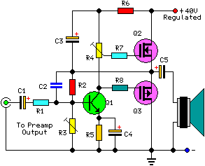 Power Amplifier Parts:
- R1 = 2K2 1/4W Resistor
- R2 = 27K 1/4W Resistor
- R3 = 2K2 1/2W Trimmers Cermet
- R4 = 2K2 1/2W Trimmers Cermet
- R5 = 100R 1/4W Resistor
- R6 = 1K 1/4W Resistor
- R7 = 330R 1/4W Resistors
- R8 = 330R 1/4W Resistors
- C1 = 22µF 25V Electrolytic Capacitor
- C2 = 47pF 63V Polystyrene or Ceramic Capacitor
- C3 = 100µF 50V Electrolytic Capacitors
- C4 = 100µF 50V Electrolytic Capacitors
- C5 = 2200µF 50V Electrolytic Capacitor
- Q1 = BC550C 45V 100mA Low noise High gain NPN Transistor
- Q2 = IRF530 100V 14A N-Channel Hexfet Transistor (or MTP12N10)
- Q3 = IRF9530 100V 12A P-Channel Hexfet Transistor (or MTP12P10)
The Preamp sensitivity and overload margin were designed to cope with most modern music program sources like CD players, Tape recorders, iPods, Computer audio outputs, Tuners etc. The source selecting switches and input connectors are not shown and their number and arrangement are left to the constructor's choice. To obtain a very high input overload margin, the volume control was placed at the preamp input.
After a unity gain, impedance converter stage (Q1) a negative-feedback Baxandall-type Bass and Treble tone control stage was added. As this stage must provide some gain (about 5.6 times) a very low noise, "bootstrapped" two-transistors circuitry with FET-input was implemented. This stage features also excellent THD figures up to 4V RMS output and a low output impedance, necessary to drive properly the Mini-MosFet Power Amplifier, but can also be used for other purposes.
Circuit diagram: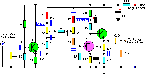 Preamplifier Parts:
- P1 = 50K - Log. Potentiometer
- P2 = 100K - Linear Potentiometers
- P3 = 100K - Linear Potentiometers
- (twin concentric-spindle dual gang for stereo)
- R1 = 220K - 1/4W Resistor
- R2 = 100K - 1/4W Resistor
- R3 = 2K7 - 1/4W Resistor
- R4 = 8K2 - 1/4W Resistors
- R5 = 8K2 - 1/4W Resistors
- R6 = 4K7 - 1/4W Resistor
- R7 = 2K2 - 1/4W Resistors
- R8 = 2K2 - 1/4W Resistors
- R9 = 2M2 - 1/4W Resistor
- R10 = 47K - 1/4W Resistor
- R11 = 47K - 1/4W Resistor
- R12 = 33K - 1/4W Resistor
- R13 = 2K2 - 1/4W Resistors
- R14 = 470R - 1/4W Resistor
- R15 = 10K - 1/4W Resistor
- R16 = 3K3 - 1/4W Resistor (See Notes)
- C1 = 470nF - 63V Polyester Capacitors
- C2 = 470nF - 63V Polyester Capacitors
- C3 = 47nF - 63V Polyester Capacitors
- C4 = 47nF - 63V Polyester Capacitors
- C5 = 6n8 - 63V Polyester Capacitors
- C6 = 6n8 - 63V Polyester Capacitors
- C7 = 10µF - 63V Electrolytic Capacitor
- C8 = 22µF - 25V Electrolytic Capacitors
- C9 = 470nF - 63V Polyester Capacitors
- C10 = 22µF - 25V Electrolytic Capacitors
- C11 = 470µF - 25V Electrolytic Capacitor (See Notes)
- Q1 = BC550C - 45V 100mA Low noise High gain NPN Transistors
- Q2 = 2N3819 - General-purpose N-Channel FET
- Q3 = BC550C - 45V 100mA Low noise High gain NPN Transistors
A very good and powerful Regulated Power Supply section was implemented by simply adding a PNP power transistor to the excellent LM317T adjustable regulator chip. In this way this circuit was able to deliver much more than the power required to drive two Mini-MosFet amplifiers to full output (at least 2Amp @ 40V into 4 Ohm load) without any appreciable effort.
Circuit diagram: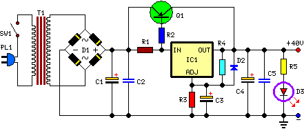 Power Supply Parts:
- R1 = 3R9 - 2W Resistor
- R2 = 22R - 1/4W Resistor
- R3 = 6K8 - 1/4W Resistor
- R4 = 220R - 1/4W Resistor
- R5 = 4K7 - 1/2W Resistor
- C1 = 4700µF - 50V Electrolytic Capacitor
- C2 = 100nF - 63V Polyester Capacitors
- C3 = 10µF - 63V Electrolytic Capacitor
- C4 = 220µF - 50V Electrolytic Capacitor
- C5 = 100nF - 63V Polyester Capacitors
- D1 = Diode bridge - 100V 4A
- D2 = 1N4002 - 200V 1A Diode
- D3 = LED - Any type and color
- SW2 = SPST - Mains switch
- IC1 = LM317T - 3-Terminal Adjustable Regulator
- PL1 = Male Mains plug with cord
- Q1 = TIP42A - 60V 6A PNP Transistor
- T1 = 230V Primary, 35-36V (Center-tapped) Secondary,
- 50-75VA Mains transformer (See Notes)
- Output power: 18 Watt RMS into 8 Ohm (1KHz sine wave) - 30 Watt RMS into 4 Ohm
- Input sensitivity of the complete Amplifier: 160mV RMS for full output
- Power Amplifier Input sensitivity: 900mV RMS for full output
- Power Amplifier Frequency response @ 1W RMS: flat from 40Hz to 20KHz, -0.7dB @ 30Hz, -1.7dB @ 20Hz
- Power Amplifier Total harmonic distortion @ 1KHz: 100mW 0.04% 1W 0.04% 10W 0.06% 18W 0.08%
- Power Amplifier Total harmonic distortion @10KHz: 100mW 0.02% 1W 0.02% 10W 0.05% 18W 0.12% Unconditionally stable on capacitive loads
- Preamp Maximum output voltage: 4V RMS
- Preamp Frequency response: flat from 20Hz to 20KHz
- Preamp Total harmonic distortion @ 1KHz: 1V RMS 0.007% 3V RMS 0.035%
- Preamp Total harmonic distortion @10KHz: 1V RMS 0.007% 3V RMS 0.02%
- Bass control frequency range referred to 1KHz: ±20dB @ 40Hz
- Treble control frequency range referred to 1KHz: +18dB/-20dB @ 20KHz