


")

The proposed detector is designed for "long" relatively search large items. It's built on a simple scheme without discriminator by type metals. The device is simple to manufacture.
Depth of detection is:
- the gun - 0.5 m;
- helmet -1 m;
- the bucket is 1.5 m.
Structural scheme
The structural scheme is shown in Fig. 4. It consists of several functional blocks.
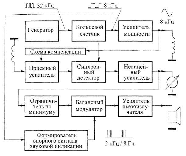
Fig. 4. Block diagram of the detector according to the principle of "transmit-receive"
The generator is a source of rectangular pulses, of which the future is formed by the signal of the radiant coil. The same signal used to signal an audible indication. The signal generator is divided in frequency by 4 using ring counter on the triggers. On ring the schema of the meter is made to its output to form two signals are shifted relative to each other in phase by 90°. Rectangular signal (square wave) is supplied from the first output of the ring counter to the input of the amplifier power load which is a resonant circuit with a radiating coil. In type power amplifier is a Converter "voltage-current", to prevent overloading of the output stage the change of polarity of the input rectangular signal of the power amplifier. The receiving amplifier amplifies the signal from the receive coil. In the take-up spool in addition to useful also penetrates and spurious signals, due to the imperfection of the system design of the coils of the metal detector, conductivity of the soil and other causes.
To remedy is compensation scheme. The meaning is that the signal of the receiving amplifier is mixed, some portion of the signal with the output oscillating circuit so as to minimize (ideally to bring to zero) the output signal of the synchronous detector in the absence of near sensor metallic objects. Setting compensation is performed by using adjustment of the potentiometer.
Synchronous detector converts the useful AC signal coming from the output the receiving amplifier, a constant signal. An important feature of synchronous the detector provides the possibility of separating the useful signal against the background noise and interference, significantly higher than the useful signal amplitude. The reference signal synchronous detector is taken from the second output of the ring counter, the signal which has a phase shift relative to the first output by 90°. Dynamic the range of variation of the desired signal at the output of the receive coil, and the output of the synchronous detector is very wide. To a display device - pointer instrument or a sound indicator equally well recorded as very weak signals and very (for example, 100 times) stronger signals, you must have the device comprises a device that compresses the dynamic range. Such device is a nonlinear amplifier, the amplitude which approaches logarithmic. To the output of the nonlinear amplifier connected arrow measuring device.
The formation of a sound signal the display begins with the limiter at a minimum, i.e., a block having a zone insensitivity to small signals. This means that the audible indication is included only for signals exceeding the amplitude threshold. Thus, weak signals associated mainly with the movement of the device and its mechanical deformations, do not irritate the ear. The shaper reference signal sound indication forms a bundle of rectangular pulses at 2 kHz with frequency of recurrence packs of 8 Hz. By using a balanced modulator this reference the signal is multiplied with the output signal of the limiter at a minimum, forming in this the image signal of the desired shape and the desired amplitude. The amplifier system increases the amplitude of the signal sent to the transducer - system.
Schematic diagram
Schematic diagram developed by the author of the detector according to the principle "transmit-receive" is shown in Fig. 5 - the input block and in Fig. 6 - block display. The division into blocks is arbitrary and does not reflect the peculiarities of the design.
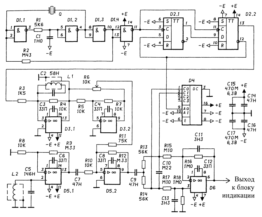
Fig. 5. A circuit diagram of the input unit of the metal detector by the principle of "transmit-receive" (click to enlarge)
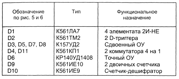
Generator
The generator is assembled on the logical elements 2I-NOT D1.1-D1.4. The oscillator frequency stable or crystal / ceramic resonator with resonant Q a frequency of 215 Hz 32 kHz ("quartz clock"). The circuit R1C1 prevents the excitation generator at the highest harmonics. Through the resistor R2 is shorted circuit environment, through the resonator Q - chain PIC. The generator is simple, low quiescent current from the power source, reliably operates with supply voltage of 3…15 V, no contains trimmer items and too high resistance resistors. Output the oscillator frequency is about 32 kHz.
A ring counter
A ring counter has two functions. First, he divides the oscillator frequency 4, up to a frequency of 8 kHz. Secondly, it generates two signals, shifted one relative to the other by 90° in phase. One signal is used for excitation oscillating circuit with the emitting coil, and the other as a reference signal of the synchronous detector. A ring counter is a two D-flip-flop D2.1 and D2.2, ring closed with inversion of the signal on the ring. The clock signal is common to both triggers. Any output signal of the first trigger D2.1 has a phase shift of plus or minus a quarter of a period (i.e., 90°) with respect to any of the output signal of the second flip-flop D2.2.
Power amplifier
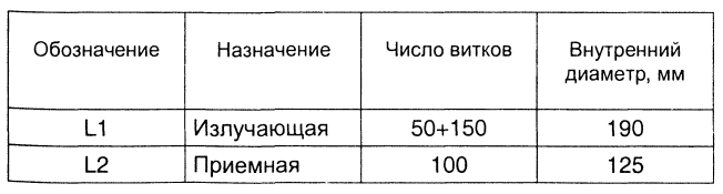
The power amplifier is assembled on the operational amplifier (op-amp) D3.1. Vibrating the circuit from the generating coil formed elements L1C2. The parameters of the coil inductance is shown in table. 2. Mark the wires - PELSHO of 0.44.
Table 2. The parameters of the inductors sensor
In the circuit OS of the amplifier output oscillating circuit is enabled only 25%, thanks to the effects from the 50th round of the radiating coil L1. This allows you to increase the amplitude of the current in the coil at an acceptable precision capacitance value of the capacitor C2.
The value of the alternating current in the coil is set by resistor R3. This resistor should to have a minimum value, but such that the OS of the power amplifier does not get mode limits output current (40 mA) or, - most likely with the recommended parameters of the inductors L1, - voltage (±3.5 V when the voltage of batteries ±4.5 V). For to ensure that there are no mode restrictions, it is enough to check oscilloscope the waveform at the output of op-amp D3.1. During normal operation of the amplifier the output should be a signal, approaching in form to a sine wave. The peaks of the sine waves should have a smooth form and must not be cut. Chain correction Oh D3.1 consists of correcting capacitor C3 is a capacitance of 33 pF.
The receiving amplifier
The receiving amplifier - two-stage. The first stage is performed at the OS D5.1. It has a high input impedance due to consistent environmental protection for voltage. This prevents loss of signal due to the shunt resonant circuit L2C5 input impedance of the amplifier. The gain of the first stage voltage is: Ki = (R9/R8) + 1 = 34. The correction circuit D5 Oh.1 consists of corrective capacity of the capacitor C6 33 pF.
The second stage of the receiving amplifier is implemented at the OS D5.2 parallel with environmental protection for voltage. The input impedance of the second stage: Rin = R10 = 10 kω - not so critical as the first, due to discoonect its source. Separation capacitor C7 not only prevents the accumulation of static error the amplifier stages, but also adjusts its phase response. The capacitance of the capacitor is selected such that the generated chain C7R10 phase leadership at the operating frequency of 8 kHz compensated for the delay in phase caused by the finite speed D5 Oh.1 and D5.2.
The second stage of the receiving amplifier, thanks to its schema, makes it easy to implement the summing (mixing) of the signal from the compensation scheme through the resistor R11. The gain of the second cascade voltage useful signal is: Ki = - R12/R10 = -33, and the compensating voltage signal: Kik = - R12/R11 = - 4. The correction circuit D5 Oh.2 consists of corrective capacitor C8 capacitance of 33 pF.
The stabilization scheme
The compensation scheme implemented at the OS D3.2 and represents the inverter CI = - R7/R5 = -1. The adjusting potentiometer R6 is connected between the input and output of this inverter and allows you to remove the signal lying in the range [-1,+1] output from voltage Oh D3.1. The output signal of the compensation scheme with the engine adjustment potentiometer R6 is supplied to the compensation input of the second amplifier stage receiving amplifier (resistor R11).
Adjustment of potentiometer R6 achieve zero value at the output of the synchronous detector that approximates compensation penetrated into the reception room the coil of the unwanted signal. The correction circuit Oh D3.2 consists of corrective capacitor C4 is the capacitance of 33 pF.
Synchronous detector
Synchronous detector consists of a balanced modulator, an integrating circuit and the amplifier constant from (oops). The balanced modulator is implemented on the basis of multifunction switch D4, made by integrated technology complementary field-effect transistors as discrete governing valves, and analog switches. The switch operates as analog switch. With a frequency of 8 kHz it alternately closes on a common bus the outputs of the "triangle" of the integrating circuit consisting of resistors R13 and R14 and capacitor C10. The reference frequency signal is fed to balanced modulator with one of the outputs of the ring counter.
The signal to the input of the "triangle" of the integrating circuit is fed through a separation capacitor C9 from the output of the receiving amplifier. The time constant of the integrating chain t = R13*C10 = R14*C10. It should be, on the one hand, as much as possible so as much as possible to weaken the influence of noise and interference. On the other hand, it is not exceed a certain limit, when the inertia of the integrating circuit prevents tracking of rapid changes in the amplitude of the useful signal.
The greatest rate of change of the amplitude of the useful signal can be described some minimum time that can happen is the change (from the steady-state value to the maximum deviation) when the motion sensor of the detector relative to the metal object. It is obvious that the maximum the rate of change of the amplitude of the useful signal will be observed when the maximum vehicle speed sensor. It can reach 5 m/s for "pendulum" movement of the sensor rod. The time changes of the amplitude of the useful the signal can be estimated as the ratio of the base sensor to the speed of movement. Putting the minimum value of the base of the sensor, equal to 0.2 m, obtain the minimum time changes in the amplitude of the useful signal is 40 MS. This is several times more than the time constant of the integrating circuit for the selected values of resistors R13, R14 and capacitor C10. Consequently, the inertia of the integrating circuit is not will distort the dynamics of even the fastest of all possible changes of the amplitude useful signal from the sensor of the detector.
The output signal of the integrating circuit is removed from the capacitor CIO. Since the last two plates are "floating potential", oops is a differential amplifier, made at the OS D6. In addition to the gain constant of the signal, the COC performs the function of a lowpass filter (LPF), additionally debilitating unwanted high-frequency components at the output a synchronous detector connected mainly with the imperfection balanced modulator.
The LPF is implemented by capacitors C11, C13. Unlike other nodes metal detector, Oh oops its parameters should be close to that precision Oh. Primarily, this refers to the magnitude of the input current, the magnitude of offset voltage and the magnitude of the temperature drift of the offset voltage. A good option that combines good properties and relative availability, is the OS type COD (or CRUD). The correction circuit OS D6 consists of corrective capacitor C12 capacitance of 33 pF.
Nonlinear amplifier
Nonlinear amplifier is implemented at the OS D7.1 with nonlinear OOS voltage. Nonlinear OOS realized by a dipole consisting of diodes VD1-VD8 and resistors R20-R24. The amplitude characteristic of the nonlinear amplifier approaching logarithmic. She is a piecewise linear, with four breakpoints for each polarity, the logarithmic approximation dependencies. Thanks to the smooth shape of the current-voltage characteristics of diodes the amplitude characteristic of the nonlinear amplifier is smoothed at the point of fracture. Small-signal gain of the nonlinear amplifier voltage is: Kik = - (R23+R24)/R19 = -100. With the growth of the amplitude of the input signal the gain decreases. Differential gain for large signal is: dUвых/dUвх = - R24/R19 = = -1. To the output of the nonlinear amplifier switches connected measuring device - microammeter with consistently included additional resistor R25. As the voltage on the output of the synchronous detector may be of any polarity (depending on the phase shift between its reference and input signals), microammeter used with zero in the middle of the scale. Thus, the pointer instrument has a range of display -100… 0 … +100 μa. The correction circuit D7 Oh.1 consists of corrective capacitor C18 capacitance of 33 pF.
The limiter on the low
Limiter the minimum is implemented at the OS D7.2 with nonlinear parallel EP on voltage Nonlinearity lies in the input dipole and consists of two antiparallel diodes VD9, VD10 and resistor R26.
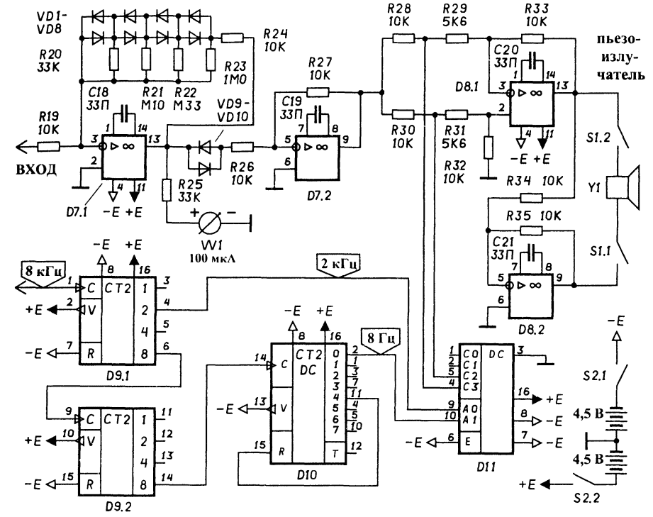
Fig. 6. A circuit diagram of a display unit of the metal detector by the principle of "transmit-receive" (click to enlarge)
The formation of a sound signal readout from the output signal of the nonlinear amplifier begins with another adjustment of the amplitude of the amplification path. In this case there is a deadband in the region of small signals. This means that the audible indication is activated only for signals exceeding a certain threshold. This threshold is determined
the direct voltage of the diodes VD9, VD10 and is about 0.5 V. Thus, weak signals associated mainly with the movement of the device and its mechanical deformations are clipped and do not irritate the ear.
The small-signal gain of the limiter at a minimum equal to zero. Differential gain voltage for large signal is: dUвых/dUвх = - R27/R26 = -1. The correction circuit D7 Oh.2 consists of corrective capacitor C19 a capacitance of 33 pF.
Balanced modulator
The signal is an audible indication is generated as follows. Constant or slowly changing the signal at the output of the limiter at a minimum is multiplied with the reference the signal is an audible indication. The reference signal sets the form for the beep and the output signal of the limiter on the low - amplitude. The multiplication of two signals by using balanced modulator. It is implemented on multifunction switch D11 working as analog switches, and Oh D8.1. The transmission coefficient of the device is equal to +1 when the open key and -1 in closed loop operation. The correction circuit D8 Oh.1 comprises a correction capacitor C20 capacitance of 33 pF.
The shaper reference signal
The shaper reference signal is implemented on the binary counter and D9 the counter-decoder D10. The D9 counter divides the frequency of 8 kHz output from the ring counter up to a frequency of 2 kHz and 32 Hz. A signal with a frequency of 2 kHz is supplied to Jr. the address bits AO multifunction switch D11, thus asking a beep tone is most sensitive to the human ear frequency. This the signal will affect the analog switch balanced modulator only when on the highest bit of the address A1 of the multi-function switch D11 will be a logical 1. When a logical zero on A1 analog switch the balanced modulator is open all the time.
The alarm sound indication of an intermittent, less fatigued hearing. To do this, use the counter-decoder D10, which is driven by a clock a frequency of 32 Hz from the output of the binary counter D9 and generates at its output a square signal with a frequency of 8 Hz and a ratio of the duration of the logical one and logic zero, equal to 1/3. The output signal of the counter-decoder D10 is supplied to the MSB of the address A1 of the multi-function switch D11, periodically interrupting the formation of tonal parcels in the balanced modulator.
The amplifier system
The amplifier system is implemented at the OS D8.2. He is a inverter gain voltage Ki = - 1. The load of the amplifier system is included in a bridge circuit between the outputs D8 Oh.1 and D8.2. It allows twice to increase the amplitude of the output voltage at the load. A switch S is used to disable an audible indication (e.g., how to configure). The correction circuit D8 Oh.2 consists of correcting capacitor C21 the capacitance of 33 pF.
Types of parts and design
The types of chips are shown in table. 3. Instead of chips series C you can use chipset series C. You can try to apply some chips series C and foreign counterparts.
Table 3. The types of chips
Dual operational amplifiers (op amps) series C can be replaced by any similar the parameters of a single General purpose OS (with appropriate changes in the Pinout and correction circuits), although the use of dual OS easier (increases the packing density).
Operational amplifier synchronous detector D6, as indicated above, its parameters should be close to precision op amp. In addition to the type specified in the table will fit COD, OD. You can use the OS COD, OD, CRUD in the corresponding switching circuit.
To applied in the circuit of the detector resistors are not required special requirements. They should be of sturdy construction and be easy to assemble. The nominal power dissipation of 0.125…0.25 W.
The compensation potentiometer R6 desirable multi-turn type SP5-44 or with Vernier tuning type SP5-35. You can do the usual potentiometers of all kinds. In this case, it is desirable to use two. One for coarse adjustment, nominal value of 10 ohms included in accordance with the scheme. Another for the exact adjustment connected in the circuit of the rheostat in the gap one of the extreme conclusions the first potentiometer, the value 0,5…1 kOhm.
Capacitors C15, C17 electrolytic. Recommended types - C50-29, K50-35, K53-1, K53-4 and other small. The remaining capacitors, except capacitor resonant circuits receiving and radiating coils, - ceramic type K10-7 (up to nomination PA 68 nF) and metal film type K73-17 (the values above 68 pF). Capacitors circuits - C2 and C5 - special. To them high demands are placed on accuracy and thermal stability. Each the condenser consists of several (5…10 pieces) capacitors included in parallel. The set of contours in the resonance occurs by adjusting the number capacitors and their value. Recommended type of capacitors K10-43. Their group on the thermal stability of refraction (i.e., approximately zero TKE). Possible the use of precision capacitors and other types, such as K71-7. In the end all, you can try to use the old thermostable mica capacitors with silver plates type CSR or polystyrene capacitors.
Diodes VD1-VD10 type KD521, KD522 or similar low-power silicon.
Microammeter may be of any type, designed for a current of 100 μa with a zero in the middle scale. Convenient compact microammeter, for example, type M.
Quartz resonator Q is any compact quartz clock (similar quartz crystals are used in portable electronic games).
Power switch - any type of compact. The battery - type 3R12 (international designation) and "square" (our).
The piezo oscillator Y1 - can be type LU1-SP. Good results are obtained when the use of pied - posluzitelja import of phones are coming in huge amounts "to the dump" in the manufacture of phones with caller ID).
The device design can be arbitrary. It it is desirable to consider the recommendations set out below and in paragraphs dedicated sensors and hull designs.
External view of the device shown in Fig. 7.
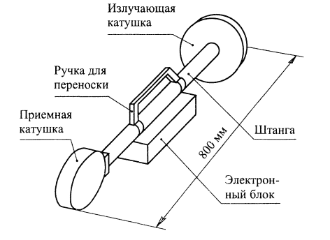
Fig. 7. General view of the detector, a transmission-reception"
In type sensor proposed the detector applies to sensors with perpendicular axes. The sensor coil made from fiberglass with epoxy glue. The same glue filled coil windings together with their fittings electric screens. Rod the metal detector is made of a pipe of aluminum alloy (AGSM, or AMGM D16T) 48 mm diameter and with a wall thickness of 2…3 mm. Coils are glued to the rod epoxy glue: coaxial (radiant) - using transient amplifying of the sleeve perpendicular to the axis of the rod (reception) - with the help of suitable shape adapter.
These accessory parts are made of fiberglass. Case the electronic unit is made of foil fiberglass by brazing. The connection of the coils of the sensor electronic unit is shielded wire with external insulation and padded inside rod. Screens of this line is connected to a common bus wire on the circuit Board of the electronic part of the device, where also connect the screen to the housing in the form of a foil and rod. Outside the colored device nitroemalyu.
PCB electronic part of the detector can be manufactured by any of traditional methods, it is convenient to use a ready breadboard PCB under the DIP IC packages (pitch 2.5 mm).
The establishment of the device
To establish this device is recommended in the following sequence.
1. To verify the correctness of installation of the power scheme. To ensure the absence of short circuits between adjacent conductors of the circuit Board, adjacent legs of the chips, etc.
2. Connect battery or a bipolar power source, strictly observing polarity. Turn the unit on and measure current consumption. It needs to be about 20 mA for each power bus. Sharp deviation of measured values from the specified value indicates a wrong or faulty installation chips.
3. Verify generator output net of a square wave with a frequency of about 32 kHz.
4. To verify the outputs of the triggers of D2 square wave with a frequency of about 8 kHz.
5. The selection of the capacitor 02 to set the output circuit L1C2 in resonance. In the simplest case is the maximum amplitude voltage (about 10 V), and more precisely zero-phase voltage shift circuit is relatively the square wave at the output 12 of the flip-flop D2.
6. To confirm operability of the receiving amplifier. To configure its input oscillating circuit L2C5 in resonance. As the input signal is enough of the parasitic signal penetrating from the radiating coil. Tune in resonance, as for the output circuit is carried out by Podpaly or removal the required number of capacitors of suitable values of.
7. To ensure compensation of the parasitic signal of the potentiometer R6. To do this, first oscilloscope control the D5 output of op-amp.2. During rotation axis potentiometer R6 amplitude signal with a frequency of 8 kHz at the output of op-amp D5.2 to change and in one of the middle positions of the R6 engine this amplitude will be minimum. Next you should monitor the output of the synchronous detector output Oh D6. During the rotation of the axis of the potentiometer R6, the constant level signal at the output Oh D6 should vary from a maximum value of +3.5 V to a minimum is 3.5 In or Vice versa. This transition is quite sharp and that his "catch", it is convenient to use the fine tuning mentioned above. Setting is the setting of a potentiometer R6, the voltage at the output of op-amp D6 equal to zero.
Attention! The setting of potentiometer R6 is needed in the absence of close coils sensor detector large metal objects, including measuring devices! Otherwise, when you move or when you move sensor about them the device will be upset, and in the presence of large metal objects near the sensor to set the output voltage of the synchronous detector in zero will fail. On compensation, see also the paragraph on possible modifications.
8. Ensure work of a nonlinear amplifier. The easiest way - visually. Microammeter should respond to the configuration process, produce potentiometer R6. At a certain position of the R6 engine the needle of the microammeter should be set to zero. The farther the needle of the microammeter is from zero, the weaker must respond microammeter to the rotation of the R6 engine.
It may well be that adverse electromagnetic environment will make it difficult adjustment of the device. In this case, the needle of the microammeter will do chaotic or periodic oscillations when approaching the arm R6 to that position in which there should be a compensation signal. Described unwelcome phenomenon is explained by the interference of the higher harmonics of 50 Hz to the take-up spool. At a considerable distance from the wires with electricity fluctuations of the arrow when you configure must be absent.
9. Make sure that the nodes that form the audio signal. To pay attention to the presence of small dead zones in the sound signal near zero on the scale of the microammeter.
If you are having problems and deviations in the behavior of individual nodes the metal detector should act according to the standard technique:
- to verify the absence of self-excitation Oh;
- check modes OS DC;
- signals and logic levels of the inputs/outputs of digital circuits, etc., etc.
Possible modifications
The device scheme is quite simple and that is why we can only go on further improvements. These include:
1. Adding additional compensation potentiometer R6* included in parallel with R6 at conclusions. The slider of this potentiometer is connected through capacitor 510 pF (need to be clarified experimentally) to the inverting input 5 D5 Oh.2. In this configuration will have two degrees of freedom when compensating the parasitic signal (sine and cosine) that can help configuring the device for use with considerable temperature variations sensor, with high ground mineralization, etc.
2. Adding additional channels a visual indication that contains synchronous detector, a nonlinear amplifier and a microammeter. The reference signal synchronous detector of an additional channel is taken with a shift of a quarter period relative to a reference signal of the main channel (from any other way out trigger ring counter). Having some experience of search, it is possible according to the testimony of two switch devices to understand the nature of the detected object, i.e. to work no worse than electronic discriminator.
3. Adding a protective diode connected in reverse polarity in parallel power sources. When there is an error in the polarity of the batteries in this case it is guaranteed that the diagram of the detector will not be affected (although, if time does not react completely discharged incorrectly battery included). Include diodes in series with the power rails is not recommended, as in this case they will go to waste 0,3…0,6 In precious voltage power supplies. The type of protective diodes - CD, CD, CD, etc.
Author: A. I. Shchedrin