


")

In Amateur practice it is often necessary to obtain two or more voltages to power the different stages of a single device. A simple example of this is the power application specific integrated circuits (voltage 5…9 and 12…15 V). In order not "procreating" power supplies and simple to use transformers with one a secondary winding (provided that the powered device does not require a large current), you can take the easy way out and get a few of the stress from one source. This approach will also save you space in the body of the device and the cost of the transformer, which is usually proportional to its power and the number of windings.
For example, to get twice the voltage from transformer power supply simply, if the rectifier is formed by the half-wave circuit, or network the transformer has a secondary winding with a branch of the middle. Such cases repeatedly described in the literature. But when the rectifier is formed on the pavement the scheme (which is most common in practice), it is possible to obtain twice the voltage possible using the scheme presented in Fig. 1.
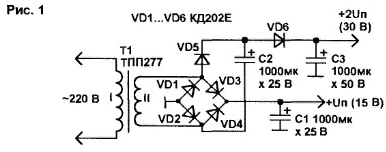
Bridge rectifier VD1…VD4 and a smoothing capacitor C1 form a the "classic" power source with an output voltage Un. Feature schema - additional channel voltage doubling assembled elements C2, VD5, VD6, C3.
Positive half wave voltage from the secondary winding of the transformer T1 through diode VD5 charges the capacitor C2. During the negative half-wave diode VD5 closed, and the capacitor C2 is connected in series with the secondary winding T1, and the voltage on the capacitor and the winding of T1 is formed. From this the voltage across the diode VD6 charging the capacitor C3, so it turns out close to twice the voltage.
When connecting the load voltage is reduced (the higher the load current, the less voltage). The load current of channel doubling flows through the diode VD1, General the wire and the capacitor C2. As a result, through the diode VD1 total current flowing (main channel and secondary). This should be considered when selecting diodes and the transformer for the future power source.
The proposed scheme source voltage doubler fits as verified option to power relatively simple devices with low current consumption (band - 1). The channels in this scheme depend on each other, and when the increase of the load current in the main channel decreases the tension in additional even at its minimum load. Therefore, at high currents better to use the classical scheme with two step-down transformer windings and a separate rectifiers.
The second option of increasing the voltage is the use of electronic the multipliers. An illustrative example of the multiplier in household appliances is the multiplier high voltage supply of a kinescope in a television receiver. On such the same principle is used for the multipliers, the input of which receives pulses voltage.
A simple example of the multiplier is the circuit shown in Fig. 2.
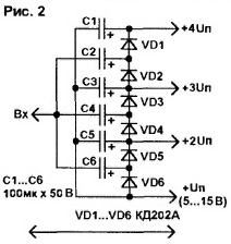
The input served pulses of any shape with a repetition rate of f=10…12 kHz and a duty cycle 0=2…3. Such pulses produces virtually any generator, built by the classical scheme for TTL or The mos IC. However, given the low load capacity of these circuits, the output of the generator is necessary to include a buffer amplifier (emitter a repeater or more elements of the chip, in parallel). The amplitude of the input signal UBX should not be less than 5 V. Since such multiplier obviously designed for a small output current, diodes VD1 VD6… used types KD521, KD522, D, D and similar. Oxide capacitors - type K50-24 and similar.
The output current of a given node will not exceed the output current of the generator, so this the voltage multiplier is used to supply only some of the chips or low-voltage cascades devices requiring high voltage. The dependence output voltage (Un) of the output current is inversely proportional to (the higher Un. the smaller the output current). Maximum output current for output doubling (2Un) in this scheme is 40 mA at Un=6, to exit at the same 3Un the voltage U" - 48 mA, 4Un - 55 mA. Maximum output current is at Un=15 In output 2Un - 10 mA, 3Un - 5 mA, 4Un to 2.5 mA.
Similarly, on the basis of this scheme receive a negative multiplier voltage. The difference is that all the diodes are included and Vice versa changes the polarity of capacitors (Fig. 3).
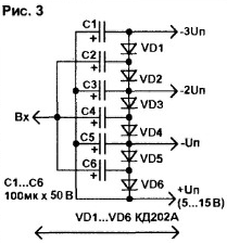
In practice it is found that negative voltage multiplier relative to the base will not exceed-3Un. The other two (lower) output voltage will be -2Un and-Un. Get in this case, the voltage-4Un without schema changes are not manages.
Author: A. Kashkarov, St.-Petersburg