


")

Main technical characteristics power supply: the power supply voltage - 200…240V, output voltage - ±25 V, 20 V and 10 V at load currents, respectively, 3 A, 1 A and 3 A; efficiency of 0.75.
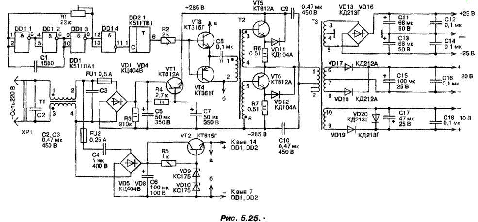
Schematic diagram of the device it is shown in Fig. 5.25.
(click to enlarge)
Network filter do the elements C2, T1, C3 Rectifier voltage Converter - full-wave bridge diodes VD1…VD4, transistor filter formed by the elements R3, C5, R4, VT1, C7. It reduces the ripple of the rectified voltage with a frequency of 100 Hz, what is necessary to prevent modulation of their rectangular voltage high-frequency transducer. The latter transistors VT5, VT6. Through step-down transformer T3, the output voltage is fed to a full-wave rectifiers VD13, VD16; VD17, VD20. Pulsation of the rectified voltages smooth capacitors C14, C18.
The master oscillator is assembled on the elements of mirhashemi DD1. Trimmer R1 the repetition frequency of pulses can be varied in the range from 100 to 200 kHz. The trigger DD2.1 produces a pulse with a more steep fronts and half the repetition rate. With the drive voltage generator is connected through the complementary emitter follower transistors VT3, VT4 and transformer T2. Power to the master oscillator is fed through a rectifier (VD5…VD8) and a voltage regulator (VT2, R5, VD9, VD10). The excess of the mains voltage extinguishes the capacitor C4.
The power supply may be used any suitable dimensions and the parameters of resistors and capacitors. Instead of transistors you can apply CTA CTA or CTB. Static coefficients of current transfer transistors VT5, VT6 should be about the same. Replace chip series C any other not recommended because they are less exposed to high-frequency interference and allow you to get pretty big (about 13 In) wingspan the pulses at the output of the trigger.
In a pinch you can use a series ICS K155, but this will require additional amplification of the pulses applied to the bases of transistors VT3, VT4. You should not replace the diodes CDG and CDA, as they have relatively high cut-off frequency (about 100 kHz), allowing you to select the same the frequency conversion and, as a consequence, reduces the size of the output of the transformer. T3 and raise the efficiency of the power supply.
Transformer network filter T1 is made on the annular magnetic core size CHH of ferrite. MNS, both windings contain 17 coils of the wire. MGTF is 0.5. The magnetic circuit of the transformer T2 from Khh ferrite. MN-1, all windings are wound in his three wires (PELSHO 0,12) and contain 90 turns. In the output transformer T3 used magnetic CHH of the same material. Its winding 1-2, 3-4-5 and 9-10 contain, accordingly, 30+5+5; 5+5 and 2 turns of PEV-2-1,0; winding contains 6-7-8 4+4 spiral of PEV-1 to 0.6. All windings are evenly distributed along the ring and carefully fix, and to exclude winding circuits are separated from one another PTFE film. Power transistors VT2, VT5, VT6 posted on three heat sinks with cooling surface area of 65 cm2 each.
Author: A. P. Seman