


")

Power, which consume amplifier installation sound systems for discos and small sites, reach 2…10 kW. In this case, for the output stages of amplifiers required supply voltage from ±80 ±160 (and above).
In this article offered bi-polar switching power supply (SMPS) (Fig.1), designed to power your amps concert USC. Among power devices, described in the magazine at the moment, this ARIA is the most powerful.
ARIA provides a constant bipolar output voltage which stabilized by pulse basis, and has an protection against overcurrent (protection against overheating of the components is not provided). ARIA is powered by a 3-phase network frequency of 50 Hz. The inclusion of the source in the network no output load does not lead to an accident and only has a negative impact the ratio of voltage stabilization. But it must be emphasized that normal the launch of the ARIA is performed only after first including all other units and systems of audiocomics. The frequency conversion apparatus - a relatively low (25 kHz) frequency and is caused by the powerful key properties transistors switching converters. If there is no imbalance. power factor SMPS can be up to of 0.955, which is associated with the feature operation of the rectifier Larionov zero diode and a filter having inductive reaction.
Purpose components
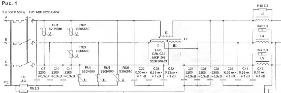
Protect the mains if any fault in the device provides 3-phase circuit breaker FU1. Varistors RU1, RU6 block transient overvoltages that occur on the network. Chokes L2 L5…together with capacitors C7, C10, C11, C22, s C32, C34, C35, S, C39, C44, s, S…S function as high-frequency jet filter, overwhelming ripple, which could take place in the supply chain. Resistors R45…R47 damp inductors L3 L5…, reducing the EMF of self-induction.
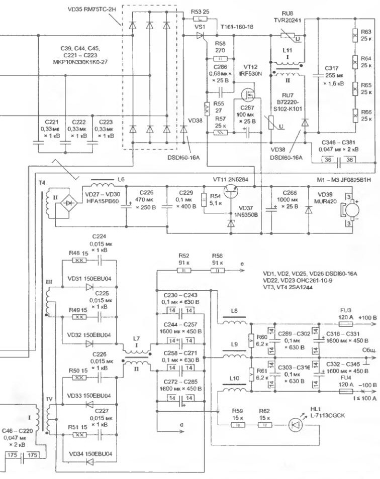
Filtered AC mains voltage supplied to the rectifier Larionov with VD35 zero diode VD36. Frequency ripple at the output is 300 Hz. The inductor L11 with small inductance needed to filter high-frequency component, able to get into the supply network, as well as to ensure that when connecting to the output of the rectifier Larionov capacitors C, S practically S decreased power factor and distortion of the shape of the phase current. Polypropylene capacitors C, S, S necessary for the normal operation of the pulse the Converter. Fixed resistors…R63 R66 drain capacitors C,S.S after completion of the operation of the device. Thanks two-winding coil II the inductor L11 and the diode VD38 happens recovery of the energy stored in the magnetic field of the inductor, back in capacitors C, S, S the power circuit of the Converter. Varistors RU7 and RU8 suppress the overvoltage pulses induced EMF of the inductor L11.
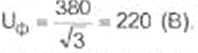
If 3-phase supply voltage is 380 V and there is no phase imbalance, the phase voltage If equal
At rated mains voltage at idle DC voltage on the output of the rectifier Larionov is

In reality, due to the fact that the rectifier diodes VD35, outdoor the thyristor VS1, the winding of the first inductor L11 and so there is a voltage drop the constant voltage applied to the switching Converter can be about 10% less.
The charge of the capacitors C, S…S at the moment of inclusion of source generates a current pulse, flowing through the bridge Larionov VD35. To the charge of the capacitors of the filter caused the current overload applied chain speed run, actuating element which acts as a thyristor VS1.
At the time of inclusion source VS1 is closed and the charge current S, S…S flows through the resistor R53, limiting his level of 22.6 And (at maximum voltage). This current is not dangerous to diodes VD35 (maximum the current consumption of the pulse Converter - about 24 A). After charging the filter capacitors shunted R53 thyristor VS1, the inclusion which occurs with a delay defined by the chain C287-R57.
Opens VS1 field-effect transistor VT12, the resistor limits the current R55 the gate electrode (resistance R55 is selected so that the current Manager electrode with the stock exceeded the trigger). The capacitor C prevents accidental firing of the thyristor from interference.
Food chain limitations of the current pulse generated by the charge of the capacitors C, S S… is supplied from parametric stabilizer R54-VD37-VT11. Capacitor S suppresses the ripple voltage. This stabilizer is powered fans M1 MOH…EMF windings which suppresses the diode VD39.
The stabilizer is connected to the pulse rectifier with LC smoothing filter on S, S, L6, VD27, VD30. The inductor L6 - demodulating. It is necessary for the voltage on the capacitors S and was S proportionally effective, not peak value of a voltage on the winding II of the transformer T4. Polypropylene capacitor C with low parasitic resistance and the shunt inductance at high frequency electrolytic capacitor C, preventing overheating of the latter.
The primary winding linear transformer T2 is connected to a network filter through fuse FU2. and the secondary winding is connected to the bridge rectifier with VD24 a smoothing filter C36, C38 Rectified voltage supplied to parametric stabilizer R34-VD13-VT9, stable the voltage from which is applied to a U-shaped filter C14-C19-L1, C23, C, C30.
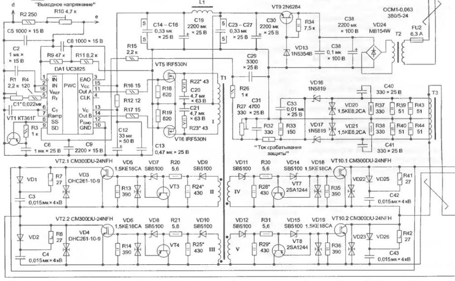
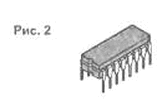
The master oscillator SMPS built on a chip DA1 - 2-stroke the controller UC3825 f.Texas Instruments (Unitrode) with chains binding". The maximum current of each of transistors key specified IC 2 pulse duration of 0.5 MS (0.5 A DC). Appointment conclusions IC in UC3825 plastic DIP-16 (Fig.2) the following:
1 - inverting input of the error amplifier,
2 - non-inverting
the input of the error amplifier,
3 - exit
the error amplifier,
4 - conclusion
frequency synchronization,
5 - customizados
resistor,
6 - condenser,
define the frequency and the duration of the pause at zero,
7 - conclusion
the sawtooth voltage;
8 - conclusion
for the organization of a "soft" launch,
9 - entrance
system lock-in current ban pulse generation;
10 - General
wire low voltage circuits of the controller;
11 output
EOL cascade "A",
12 - ground high current terminal of the cascade,
13 - conclusion for applying voltage to the final stage,
14 - output terminal of the cascade "In ",
15 - pin for connection to a power source,
16 - output
reference voltage (+5.1 V).
Resistors R2, R10, R52, R58 (Fig. 1) organized the divider output voltage of the SMPS, which is applied to the capacitor C230…S, S…S. Elements R11 C5 and increase the immunity system of automatic control. Constant voltage, falling on the resistors R2 and R10, connected to the inverting input of the amplifier the error circuits DA1. According to the reference data of the manufacturer, this voltage should be within the range -0,3 to+7 relative to the pin 10 of the chip. If the divider R2-R10 R52-R58 is served a constant voltage of 200 V, the adjustment of the resistance R10 can to achieve at pin 1 voltage DA1 and the range of +0.27 to+5.3 V (relative to the potential of the terminals 10 and 12). Should notice that the adjustment will result R10 the output voltage, and hence the voltage at inverting the input of the amplifier error signal.
System for stabilizing the output voltage does. If the output voltage SMPS for any reason increases, it also increases the voltage, coming from the frequency divider output 1 DA1. This causes a decrease in the coefficient fill generated by the chip pulses in power modules, i.e. a reduction in the duration of bipolar pulses at a constant frequency the generation. The effective voltage on the secondary windings of the pulse transformer T4 is reduced, and the DC voltage after demodulating inductor L7 applied to the capacitor C230…S, returns to the original level.
Control constant voltage is the input power of the high-frequency filter, and not at its output, as the presence of excessive phase shift would lead to the instability of the system of automatic regulation of the output voltage (instead of the negative could be positive feedback and the excitation SMPS). It is essential that the capacitor C230…S and S S… had the minimum value of the parasitic resistance and inductance.
Chain R9-C8 - corrective error signal amplifier. The reference voltage (+5.1 V) is fed directly to the non-inverting input 2 of the error amplifier. Ceramic capacitor C2 provides filtering of ripple. НоминалыR1, R4 and C1 determine the frequency of the pulses, which are produced by DA1. The capacitance C1 determines the duration of the pause ("dead time") between opposite-polarity pulses, the larger the capacitance C1, the longer dead time.
On the components C6, R3, VT1 assembled circuit soft start setpoint generator DA1. Elements R12, C12, C13 - passive filter built-in high frequency ripple and "dividing" low-power advanced circuits and high-current terminal cascade DA1. Capacitors C12 and C13 must have it is possible to lower the parasitic resistance and inductance. Capacitor C13 - the ceramic. Nominal voltage tantalum capacitor C12 should not be below 50, otherwise it can break, and tantalum capacitors usually fail with by closing the circuit.
Between the output stage circuits DA1 and chains forcing discharge of containers gate-emitter of the switching transistors of the power modules VT10 VT2 and placed driver with two MOSFET VT5 and VT6. Their purpose - umewaka pulses applied to the winding I of the matching the transformer T1. Resistors R16 and R17 delay unlocking and locking of transistors VT5 and VT6, and R18 and R19 drain their capacitance gate-source, RC-chain C20-C21 R22 and-R23 necessary for damping of the primary Polubotok of pulse transformer T1. Without them the form of control pulses transistors key modules VT10 VT2 and was would highly distorted, which would inevitably lead to disaster.
The strength of the current flowing on the primary winding of I power pulse transformer. T4, keeps track of the current transformer TK. Pulses current flowing through resistors R39, R40, R43 and R44, create them fall voltage the magnitude of which is proportional to the current of the primary winding. Speed increasing stress on these resistors reduce RC-C40 chains-R37 and C41-R38, which, moreover, contribute to fast the attenuation of spurious oscillatory processes. Bidirectional transil (transil Transient Voltage Suppression Diode) VD20 VD21 and limit the amplitude of the pulse overvoltage.
Pulses straighten Schottky diodes VD16 and VD17 loaded on SS and R33, which form a peak detector. The rectified voltage is applied to the voltage divider R27-R32 Vremenem engine setup resistor R27производится adjustment is necessary sensitivity which must have system protection operation current. The voltage divider signal overload enters multilink the filter C9-C29-C31-R15-R26 which suppresses high frequency ripple. The more capacity C9, s, C31, the higher the resistance R15 and R26 is, the more inertia has the protection system current. If it is excessively inertia, you will not be able to perform protective functions, but if too fast-acting, possible false positives.
The filtered signal voltage for overvoltage is input 9 circuits DA1, that in the event of an emergency of increasing current will provide a lock of the controller. While the voltage at pin 9 DA1 is +of 0.9 to+1.1 V relative to pin 10, there is a reduction coefficient fill pulses, and if this voltage reaches +1,25…+1.55 V, the generation of pulses is terminated. Typical time delay switch-off conclusion 9 IC UC1825, UC2825 and UC3825 is only 50 NS, and the maximum the length of the delay does not exceed 80 NS. According to the Handbook, the highest voltage that is valid to apply for entrance 9 relative to the pin 10, is +6, and this device does not exceed 3,8 V.
Matching the transformer T1, the transformer T3 and the power pulse transformer T4 provide galvanic isolation of input and output circuits of the device. Transformer T1 assumes the functions of the galvanic decoupling of the forced discharge packing containers IGBT modules VT10 VT2 and from each other and from the transistor driver. The circuit of the forced locking IGBT modules VT10 VT2 and presents four groups of components: R13, R20, R24, VD5, VD7, VD9, VT3; R14, R21, R25, VD6, VD8, VD10, VT4; R28, R30, R35, VD11, VD14, VD18, VT7; and R29, R31, R36, VD12, VD15, VD19, VT8. Resistors R20, R21, R30 and R31 need to slow down on and off of the respective transistors in power modules VT10 VT2 and, reduce the amplitude and duration of oscillatory processes. Without this there would be the danger of losing control of the IGBT-modules because of the "latch" parasitic thyristor structures caused by excessive the slew rate of the signal.
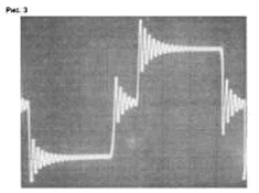
Specialists f.Роwеrех, Inc., producing power modules CM300DU-24NFH, recommend the resistance of the gate resistors in the range 1…10 Ohms. Resistors R24, R25, R28 and R29 damp spurious oscillations that occur in chains. If you remove load windings II, III, IV and V matching transformer T1 and resistors R24, R25, R28 and R29, the shape of the voltage pulses in the secondary windings this transformer takes the form shown in Fig.3 (the duration of the sweep - 5 µs/div.). Obtain pulses with such damped oscillatory processes should be avoided.
When the power source voltage Converter is applied to parasitic voltage dividers formed from tanks gate-emitter and gate-collector of the IGBT modules. If you do not limit the voltage between the gates and the emitters safe for transistor level, they break through. Voltage gate-emitter in the IGBT modules CM300DU-24NFH not exceed ±20 V, which is a common value for this class of the devices. Protection circuits the gate-emitter assume bidirectional suppressor diodes VD5, VD6, VD18 and VD19. Accelerated discharge of containers gate-emitter IGBT modules provide a bipolar p-n-p transistors VT3, VT4, VT7 and VT8, which when opened, shunt control inputs of the electronic keys. The discharge capacities gate-emitter also help resistors R13, R14, R35, R36.
Powerful suppressor diodes VD3, VD4, and VD22 VD23 protect transistors key from overvoltages. Damping chain C3-R7-VD1; C4-R8-VD2; C42-R41-VD25; C43-R42-VD26 is "snobbery". If they were absent, every time you locked keys in crystals of IGBT power modules VT10 VT2 and short-term would be allocated more power, amounts to many kilowatts, and this caused would intensive degradation of the semiconductor power transistors and, in the end all, would have resulted in failure.
Capacitors S.S prevent long-term DC magnetic bias core pulse transformer. T4, which could cause saturation of the magnetic circuit T4.
Powerful diodes VD31. VD34, shunted snobbery S-R48, C225-R49, C226-R50 and S-R51, collected two separate the output pulse rectifier. The inductor L7 is used for demodulation and group stabilization of voltages. Capacitors S230…S, S…S, S…S and inductors L8 L10…form output. U-shaped filter, which smooths out the high frequency ripple. Capacitors S230.S, S…S, S.S should have minimum parasitic resistance and inductance. Resistors R60 and R61 drain the output filter capacitors after the conclusion of the SMPS. HL1 led indicates the enabled state of the apparatus, and resistors R59 and R62 limit flowing through it current. Fuses FU3 and FU4 off the load from the output filter capacitors SMPS in case of overcurrent.
Possible replacement components
Chip 0A1 brand can UC3825 to change UC2825, UC1825 or CEO.
Customizados capacitor C1 should have a group on thermal stability of IGOS. Suitable, for example, the capacitor of the brand. K71-7. You cannot use the capacitors, which may "flicker capacity". Capacitors C3, C4, S and S in the damping circuits capacitance 15 pF and rated voltage 4 kV (direct current) is used with polypropylene dielectric brand Snubber FKP15N/4000 firm "WIMA". Their you can change the Snubber devices FKP15N/3000.
Capacitors C7, C10, C11, C34, C35, C - ceramic Yl-type, and C22, s, C32, C39, C44, s, S…S - polypropylene, metallized, X1-type. Capacitors C7, C10, C11, C34, C35, S valid use a brand DECE33J222ZC4B, and to replace such marks can DHRB34C102M2FB or K15-5 capacity 2.2 nF and a rated voltage of 6.3 kV. Capacitors C22, S, C32, C39, C44, S, S…S - MKP10N330K1K0-27 firm "WIMA" with self-extinguishing foamed body. These capacitors are interchangeable on MKP10470N/2K, MCR 1U/1.6 K or similar. You can use capacitors metallized polypropylene 0.33 µf 0.47 µf or 0.68 UF series. MCR firm "Vishay" for for a voltage of 600 VAC. Capacitors S.S with a capacity of 47 nF and rated voltage DC 2 kV - polipropilenovye high-frequency, FKP14 7N/2000 . Total the capacity of a group of 175 included in parallel capacitors is approximately 8.2 UF.
The capacitor C230, C, S, S, S…S-polypropylene high frequency brand FKP4 0.1 U/630 or MCR 0.1 U/630. These capacitors are required to possess minimal parasitic inductance and resistance. The capacitor C with the insulator metallized polypropylene - DC-LINK HC VEARTH-type. Instead the capacitor 255 UF can take the capacitor 340 UF the same type and rated voltage. Capacitors C…S - polypropylene high frequency, FKP147N/2000.
Capacitors S244, S, S, S, S, S - series NQ f. "Aihuan Technology Group". Capacitor this series capacity 1600 µf and rated voltage of 450 V withstand current pulsations of 9.8 And at a frequency of 300 Hz and a temperature of 85°C. To the amplitude of the fluctuations they did not exceed the maximum allowable value, had to combine connected in parallel capacitors in the group.
Trimming resistors R1, R10, R27 brand SP5-2B can try to change the resistors SDR-19A, SDR-39, SP5-SV, SP5-16 or SP5-22 can be replaced by resistors series PVZ3A or PVM4 firm "Murata Manufacturing". However import trimming resistors have a different number of resistors, and therefore, when replacing the need arises to adjust the resistance of fixed resistors connected in series with the trimpot.
Resistors R7, R8, R41, R42 - R (non-inductive) of the company "LAETA" in the building. TO-247. The cooling of the resistors are separate radiators HS104-50 size 100x102x24,5 mm. Resistors R48, R51 can to apply either the same brand RA, or take the SMHP series resistors power 20 W in the case of THE to-263 firms "TT electronics", or to make the 4 non-inductive resistors power of 5 watts. DC resistor R53 - wire, C5-W-50 or C5-35B. It is important that this resistor is easy withstand momentary over-current. Resistors R63, R66 - wire, C5-47C.
Variators RU1…RU6 type S20K680 brands can take B72220-S 681-K, TVR20112 or CNR20D112. Varistor RU7B72220-S102-K101 triggered when the voltage 895 DC and is able to absorb energy up to 410 j. It is permissible to change two switched in parallel varistor B72220-S681-K101 (each triggered when the voltage 895 In and can absorb energy up to 250 j). Varistor RU8 TVR20241 has the voltage at a constant current of 200 V and is capable of absorbing most energy in 108 joules. The said varistor to replace B72220-S2131-K101, JVR-20N241K, S20K130E2 or S20K150.
Diodes VD1, VD2, VD25, VD26, VD36 and VD38 brand DSDI60-16A can be exchanged for diodes DSDI60-18A manufacturer or RHRG75120, RHRU100120 f. Fairchild Semiconductor Corporation". The diodes are mounted on a separate coolers HS143-100 or similar. Bidirectional suppressor diodes VD3. VD4, and VD22 VD23 (ONS-10-9) can be replaced. ONS-s-8 or. ONS-10-10. Suitable coolers - 0171 or 0371.
Bidirectional suppressor diodes VD5, VD6, VD18 and brand VD19 1.CASE can be exchanged for CRSA or. RCES. Schottky diodes VD7…VD12, VD14, VD15 (SB5100) are replaced by MBR750. SB560, SB860 or SB860F. Zener VD13 1N5354B has the breakdown voltage of 17 V. It can be exchanged for 1SMA5930B, 1N5355B-MBR or 1N5353B. Schottky diodes VD16 and VD17 (1N5819) change 11DQ06, 11DQ10, MBR160, SB140…SB160. SB1100, SR1100, SR106 or SR180. Bidirectional diodes VD20 and VD21 (1.CA.SA) interchangeable on the protection diodes RCE.SA, RCES or 1.CASE.
Diode Assembly VD24 type MB154W can be exchanged for one of the devices BR154, BR156, BR158 or MB156W. She mounted on the cooler, such as a brand HS183 dimensions 30x50x17 mm production Kinsten Industrial".
Ultra fast diodes VD27…VD30 HFA15PB60 can be replaced by part no dsei12-06A. FES16DT. FES16FT or HFA15TB60. They are mounted on four separate cooler HS184-30 with dimensions 30x41x30 mm or similar. Ultra fast diodes VD31.VD34 150EBU04 allow in direct starting current of 150 A (at a temperature of 104°C) and can withstand most reverse voltage 400 V. the typical duration of reverse recovery 172 NS (when the direct current of 150 A, reverse voltage 200 V and 125°C). Maximum forward voltage drop across the diode is 150EBU04 1.17 V At a current of 150 A and a temperature of 125°C. These components can be changed to build HFA320NJ40C or HFA280NJ60C consisting of two diodes. It should, however, remember that the diodes have a common cathode. Valid replacement and MUR20060CT.
All four diodes (VD31…VD34) are mounted on independent coolers HS153-100 f. "Kinsten Industrial" or similar. Three-phase diode bridge VD35 brand RM75TC-2H can be exchanged for a similar bridge 160МТ160SW. A diode bridge is mounted on cooler HS153-50 or similar.
Zener brand VD37 1N5350B has the breakdown voltage of 13 V (±5%). You can replace one of the Zener 1N5351 In, BZX85C-13V or ZY13.
Diode VD39 brand MUR420 valid replace BYD1100, BYV28-100. SBYV28-200. SF22. SF54 or SB5100.
It is desirable that the led HL1 had green or blue glow. Instead of led brand L-7113CGCK can take one of the devices CIPM-1L, KPMG-1L, L-383SGWT, ARL2-5213PGC or L-1503SGC.
Low-power p-n-p transistor CTG (VT1) valid to change to other transistors of the series KT361, and similar devices. Sun 157, 158 SUN WSW, VSS.
Power modules VT10 VT2 and contain two United by the half-bridge circuit powerful IGBT with integrated boxer diodes. Transistors modules CM300DU-24NFH allow work at frequencies up to 30 kHz in hard switching at a frequency of 60…70 kHz in the resonant mode. Constant current collectors of transistors 300 And, the pulse current of 600 a, And the maximum voltage collector-emitter - 1200 (at 25°C). The highest saturation voltage collector-emitter transistors modules is 6.5 In, and its typical value is 5 V. Each the power module must be installed on a separate cooler, for example, "DAU" series IHV or IHM, and quite in length Is 300 mm. these components is permissible to use modules CM200DU-24NFHили a number discrete transistors, for example, IRGPS60B120KDP. Last I have the collector current 105 A, a pulse - 240 a, And the maximum voltage collector-emitter - 1200 (at 25°C). In the apparatus applied to those components that have been the author. When selecting transistors key it should be remembered that the allowable current collectors of the IGBT strongly decreases with increasing frequency conversion and temperature. With increasing temperature also reduced allowable power dissipation of transistors. The most current of the primary winding of the power pulse transformer. T4 approximately 24 And that also must be considered.
Transistors VT3, VT4, VT7 and VT8 (2SA1244) it is permissible to replace 2SB1202. Field MOS transistors VT5, VT6 and VT12 (IRF530N) can be changed on IRFU3910, IRF530, IRL530N or IRFI540G. Transistors VT5 and VT6 are mounted on a miniature coolers KG-331 production "Kingcooler", and the transistor VT12 - on the radiator HS115-50, HS113-50 'Kinsten Industrial" or similar the efficiency. Component VT9 brand 2N6284 permissible to change 2N6283, CTA, CTB. The transistor is mounted on the cooler HS143-150 or similar. Bipolar transistor VT11 brand 2N6284 can to change CTA. It should be mounted on the cooler HS153-50 or similar.
The thyristor VS1 brand T-160-18 mounted on the cooler 0171 or 0371. You can replace T-160-14, T-160-15, T-160-16, T261-160-18 or T-200-14.
Choke L1 - LPV2023-501KL f. "Bourns". According to the reference data, the inductance of the windings is 500 (±10%) mH, and its most soprotivlenie to 0.28 Ohms. The throttle can withstand a maximum current of 1.5 A.
The inductor L2 perform on two stacked toroidal magnetic powder iron. Kzt650-26 or Kzt650-52 size K,h,g,8 f. "Micro-metals". Winding of the inductor wound simultaneously in the three wires. Each coil should contain 18 turns and have the inductance 265 mH. As winding wire it is permissible to use a "pigtail" lived out of 10 copper wire sew-2 or PETV 0,55 mm (copper). Inductors L3 L5…perform on the toroidal powder iron cores T400-26D size CH.2x33 mm "pigtail" lived out of 10 copper wire sew-2 or with petv the diameter of each of 0.55 mm (copper). Each winding consists of 32 turns, the inductance - 265 mH.
The inductor L6 taken LPV2023-501KL f. "Bourns". He has a maximum current of 1.5 a, the coil inductance 500 (±10%) mH, and its resistivity is not more than 0.28 Ohms. Two-winding choke L7 perform on one toroidal magnetic core powder iron. Kzt650-26 or Kzt650-52 CH,9x50,8 mm Winding of the inductor is placed simultaneously in the two wires to obtain the inductance of each winding 35 µh (the number of turns of each winding - 10). Winding perform the "pigtail" wire 90 sew-2, PETV or PELSHO 0.55 mm each (on copper). Due to the fact that the output of the rectifier - full-wave rectifier, ripple the rectified voltage have a twice higher frequency relative to frequency conversion.
Inductors L8 L10…perform on the annular magnetic powder iron. Kzt650-26 or Kzt650-52 CH,9x50,8 mm Number of turns of each coil 10, and the inductance each of the inductor - 35 µh. As the winding wire is the "pigtail" from the 90 lived in diameter each of 0.62 mm.
Winding the inductor L11 is implemented on two stacked toroidal magnetic powder iron. Kzt650-26 or. Kzt650-52 size CH,9x50.8 mm production ""Micrometals"". Winding wound "pigtails" of wire 22 brands PETV or sew-2 0.55 mm ( copper). Windings, each of which has 29 of turns is wound in two wires. The inductance of each coil is about 675 µh.
Pulse transformer T1 is made on a toroidal the magnetic core of ferrite MNM-size Chg. The coil I wound folded in four wires sew-2 or PETV 0.38 mm, winding II, III, IV and V - folded twice wires of the same brand of 0.38 mm. Winding I has 130+130 of turns of the winding II, III, IV and V - 130 turns. Winding insulation perform a tape of polyester or Dacron. The inductance of the windings II, III, IV and V, and also, any of the primary Polubotok is 22 mH.
The transformer T1 can be wound on the armored core B ferrite MNM (without podstroechnik and gap). At the same winding II, III, IV and V and each of the primary Polubotok must contain at 88 turns of wire of the same brand and of the same diameter. The inductance of the windings also will not change.
Instead of a linear-phase transformer T2 of the brand. OSM -0,063 380/5-24 can take the transformer OSM 1-0,063 380/36, OSM 1-0,1 380/5-24, MSDS 1-0,16 380/5-24 or similar.
The current transformer. T3 formed on the yoke 12x15 W from manganese-zinc ferrite NM-11 or NS. The primary winding consists of at one loop, for convenience, the beam is made from wire 22 sew-2 or PETV 0.55 mm (copper). The diameters of the veins taking into account the thickness of the insulation coating is 0,62 mm To increase the dielectric strength of the insulation of the primary the winding of the current transformer is passed through a glass tube Secondary winding comprises 74+74 round two stacked solid wires of the same brands 0.33 mm (copper). To prevent saturation in the core is left non-magnetic gap thickness of 0.05 mm.
Power pulse transformer. T4 can be performed on five stacked together via insulating gasket thickness 0.05 mm sets of magnetic cores. Sh ferrite NM, designed to operate in a strong magnetic fields. With this configuration, a large portion of the windings will be shielded from environment ferrite side cores. In the magnetic circuit is useful to make a nonmagnetic the gap of 0.02+0.02 mm, which would increase the maximum allowable magnetic field strength in the core.
The use of large magnetic cores due to the conversion frequency of 25 kHz, the choice of which is associated with acceptable speed switching transistors modules VT10 VT2 and. Winding I T4 has 9 turns "pigtails" of 18 lived of PEV-2 or PETV of 0.47 mm Winding II has 1 coil of 0.47 mm Winding III and IV must be the same and consist of 2+2 turns of the Smurfs lived from 38 0.4 mm each. Between the windings need pave thin insulation (not more than 0.3 mm), but which should provide the required dielectric strength. It should be noted that winding lay this is challenging given that the window of the magnetic circuit is obtained almost completely filled. The transformer core should stick via insulating strip of mica not less than 4 radiators brand KG 370 KG or-222.
Three-phase automatic switch FU1 ABB S203 SA you can change at ABB S203R C32, Moeller SP PL6-C40/3, Moeller 3P PL6-C32/3. Fuses FU3 and FU4, calculated on the actuating current of 120 A, it is possible to apply a car from "FLOSSER", type "b" or brand. PN-2.
Fans M1 MOH…JF0825B1Н production "Jamicon Corporation" with the supply voltage of 12 V and a quiescent current of 0.19 And have dimensions 80x80x25 mm and a capacity of 1.1 m3/min permissible to replace JF0815B1H. JF0825S1H,EC8025M12SA.KF0820B1H, or KF0820S1H similar to the consuming current of 0.2 A.
Design
Electrobite the device connects to the network flexible cable of the brand. CHAT-6 3x10+1x6+1x6 (TU16.C-125-2002) or similar.
Capacitors C12, C13 should be placed in the vicinity of pins 12 and 13 of the microcontroller DA1. The length of the conductors and the length of paths should be as minimal as possible. Board with the reference generator is placed in an electromagnetic screen, electrically connected to the terminals 10 and 12 DA1. Capacitors S.S close raspalaut to each other on both sides of the long double-sided PCB, resembling the line along which the etched only 4 lanes-bus: one two side, and two opposite opposite. Capacitors C…S connected directly to the terminals of the key transistors modules VT10 VT2 and.
The snubber circuit C3-R7-VD1, C4-R8-VD2, C42-R41-VD25 and S-R42-VD26 connected directly to the terminals of the collector-emitter transistors modules VT10 VT2 and. Damping RC-circuit C40-R37, C41 -R38, C224-R48, C225-R49, S-R50 and C227-R51 are as close as possible to respective components; the current transformer T3 and the diode VD31…VD34.
Mounted coolers details establish the thermal paste brand, АЛСBG-3, CPT-8 or similar. Power a pulse transformer. T4 is placed in the path of air flow from one fans M1 MOH…because during operation of the SMPS in a long-term mode with a maximum power output of the transformer very much warming up.
The whole ARIA is escaped, the electromagnetic shield is connected to GND. Under the capacitor C8 and resistor R9, and also the connecting tracks on the opposite side of the bilateral boards it is advisable to leave neitralnuju foil, playing the part of the screen that connected to leads 10 and 12 circuits DA1.
Setting and regulation. Before you can set up need carefully check the installation and the phasing of the transformers T1, T4, chokes L2, L7 and L11, and then adjust the resistance of the trimming resistors. The resistance R27 should be maximum, and the engines resistors R1 and R10 set to the middle position. You can now proceed to unit testing apparatus, which will require an oscilloscope, laboratory power supply, multimeter, equivalent load (power resistors) and two incandescent lamps with capacity of 300 W.
For starters, you should make sure that the surge protector is operable. In the check is removed предохранительFU2 to disable auxiliary the power source of the master oscillator, and do not connect the rectifier to VD35 power strip. When the filter into the network at its output should to attend the three-phase alternating voltage of the same amplitude as at the entrance. In the absence of a reactive component of the load current consumed filter from the network should not significantly exceed 0.4 A, and the active component of the current must go to zero. Then the filter disconnect from the network and connect to it the rectifier Larionov.
Rectifier diode VD27…VD30 disconnect from the winding II pulse of the transformer. T4 and connects laboratory power supply with an output voltage 15…20 V and allowable current of at least 1 A. On the capacitor C must be a DC voltage of about 12 V, fan M1…MOH needs earn I. finally, it should open the thyristor VS1. Now laboratory power supply unit is turned off, but do not disconnect from the rectifier.
Break the chain between the connection point of the varistor RU8 inductor L11, a resistor R63, capacitors S, S, S and a connection point of the collectors of the IGBT VT2.1.VT10.1, resistors R7…R41. diodes VD1, VD3. VD22, VD25. Thus, switching Converter is disconnected from the network rectifier system speed of the charge in the capacitors of the filter. Parallel to the capacitor C is connected to a load equivalent to two lamps connected in series the filament type LONS capacity of 300 watts. During the experiment, when will a significant heating резистораR53, served the voltage at the rectifier VD27.VD30 from laboratory power supply.
After all the preparatory operations, turn your device into the network. The diode should VD36 to attend the DC voltage approximately 515 In at rated network voltage (from 463 to 565 In) when the mains voltage deviation ±10%). When this thyristor VS1 should be closed, which can be defined as an instrument, and the presence of heating resistor R53 Include laboratory power supply, and VS1 must to open, which will cause a decrease in the temperature of the resistor R53. If so, the apparatus is disconnected from the network, shut down a lab power supply and restore the connection between the condenser C and the collectors of transistors VT2.1 and VT10.1, and also the rectifier VD27…and VD30 the winding II of the transformer T4. Removed the fuse FU2 return .
Diode bridge disable VD24 from the transformer T2 and is connected to a laboratory power supply with exposed an output voltage of 20 V (19 to 24 In). The capacitor C19 C30 and should to attend the DC voltage approximately in the 15th Century To the terminals 11 and 14 circuits DA1 connect oscilloscope and using the adjusted resistor R1устанавливают the frequency of 25 kHz.
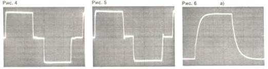
During the period must be observed in two different polarities of the pulse is rectangular in shape with steep fronts, and between pulses - protective pause (Fig.4, sensitivity 5 V/cell, the duration sweep - 5 MS/division). The duration of protective pause is selected, based on the settings of the switching transistors. It is desirable that it was not less than 2.1 μs. To change the duration of the dead time, you should take the capacitor C1 with a different capacity.
Large capacity will increase the length of the pause at the zero level, and less - on the contrary. But the adjustment of the capacitance of the capacitor C1 will change the frequency conversion, and have to re-adjust frequency trimming resistor R1.
Between the drains of transistors VT5 and VT6 must attend the voltage pulses almost the same shape as in Fig.4. Form voltage pulses on both halves of the primary winding of the matching transformer T1 shown in Fig.5 (at the time of measurement to windings II, III, IV and V are not connected load).
To check health protection circuit current otpaivaete secondary winding of the transformer current T3, and parallel to the resistors R39 and R43 is connected laboratory power supply unit with exposed 6 V so that it "+" was is connected to the anode of the diode VD16, and " - " terminals 10 and 12 DA1. The controller have to stop the waveform generation. If you connect the "+" laboratory power supply to the anode of the diode VD17 generation of pulses must also cease. Disconnect the laboratory unit and solder winding T3.
You can verify the operation of the circuit, accelerating the discharge of containers gate-emitter transistors modules VT10 VT2 and (R13-R20-R24-VD5-VD7-VD9-VT3, R14-R21-R25-VD6-VD8-VD10-VT4, R28-R30-R35-VD11-VD14-VD18-VT7 and R29-R31-R36-VD12-VD15-VD19-VT8. In the presence of these circuits, the discharge gate capacities must to occur faster than in their absence. It is useful to check the pulse shape voltage between terminals of the gate-emitter of the switching transistors of the power modules VT10 VT2 and. Without circuits of the discharge gate capacitances form of pulses shown in the waveform Fig.6A, and in the presence of these circuits in Fig.66 (sensitivity - 2/cage, scan - 0.2x50 MS/division). Both diagrams removed for a single IGBT (IGBT collector not connected to the circuit of the inverter, IGBT and the other three chain of accelerated discharge of their packing containers disabled).
A significant influence on the shape of the voltage pulses gate-emitter transistors, power modules VT10 VT2 and have the resistance of the damping resistors R24, R25, R28, R29 and chain C20-C21 R22 and-R23, you can pick up, ensuring better shape.
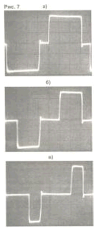
To check the pulse width impulses voltage adjustment disconnect the resistor R58 from R52 and connect the "-" laboratory power supply to point d . In parallel any of the secondary winding (II, III, IV or V) pulse the transformer T1 is connected to the oscilloscope, and resistors R20, R21, R30, R31 to the experiment may be given. Changing the output voltage of the laboratory block power from zero to 100, we see that changing the duty cycle, and their the frequency and shape remain unchanged. This is shown in the waveform (the sensitivity of the amplifier Y - 5 V/cell, scan - 5 MS/division): Fig.7a - minimum duty cycle, Fig.76-medium, and Fig.7b is a maximum. If adjusting the duty cycle occurs successfully, disable laboratory power supply and solder the resistors R20, R21, R30 and R31.
Only after the procedure can include the SMPS in the network (without connecting thereto the load). Using a trim resistor R10 set output voltage ±100 V.
Between the outputs of the SMPS -100 and +100 (after fuse FU3 and FU4) connect the equivalent load resistance of 3.6 Ohms. As the equivalent load can to use modules brake resistors series OHMEGA firm "Danotherm "or spiral of nichrome wire mounted on non-combustible base.
Rotating engine of the resistor R27, achieve actuation of the protection system and disconnect the SMPS when the load power 11,1 kW. Then take the equivalent load resistance 4 Ω, which corresponds to an output power of 10 kW. When connecting it to the unit the protection system should not be triggered. At the end of the tuning work you should check the source nutrition in long-term mode and to control the thermal conditions of the components.
Attention! During commissioning and operation of the source must comply the safety regulations.
Author: E. Moscato, Taganrog, Rostov region