


")

The article details the structure and principles of operation of the amplifying modules broadband TV antennas.
Amplifier in a television reception antenna is designed mainly to increase the sensitivity by the noise, and, second, to compensate the received signal in the coaxial cable. TVs themselves have a very large stock of their own gain, i.e., have high sensitivity, limited amplification. Worse they have a sensitivity limited by synchronization. Finally, the lowest - the sensitivity is limited by noise. Consequently, the determinant of distant reception, you should take the noise floor of a linear path, not a gain.
The effect of noise is estimated in relation signal/noise, the minimum value of which was equal to 20. For TVs third - the fifth generation of the sensitivity is limited by noise, equal to 50-100 mV. However, when signal-to-noise ratio (SNR) equal to 20, there are bad image quality and clarity only the major details. To obtain a good quality image should be submitted to the television input signal is about 4 times greater, i.e. to ensure the ratio is about 80.
The currently used cables with a characteristic impedance of 75 Ohms, depending on the design and quality of the dielectric have a linear attenuation of 0.07 and 0.18 dB/m in metre and 0.25 - 0.6 dB/m in the UHF band. Cable lengths of 2 m…4 total attenuation may be 1.2 to 2.4 dB. In this regard, the amplifier must have a gain of about 3 dB for a typical reception conditions. To it add the stock in 12…14 dB to amplify weak signals, which is necessary due to the low efficiency compact broadband receiving antennas.
Any amplifier has its own noises that are amplified along with the desired signal and degrade the signal-to-noise ratio. Therefore, the most important parameter of the amplifying element should be considered as the noise coefficient Ksh.
For a single noise assessment of multi-path exists, the adjusted noise ratio CABG, which equals the level of noise at the output divided by the total gain, i.e., CABG = coronary artery bypass grafting.o / KU. Since the output level of the noise Cs.o depends to the greatest extent from the noise of the first transistor, amplified by all subsequent stages, the noise remaining stages can be neglected. Then CABG.o= Cscu where X - noise ratio of the first transistor. Therefore, get Sh= X, i.e. given the noise factor of the amplification part is mainly determined by the noise figure of the first transistor. Hence the conclusion - the use of the active part can give a positive result when the noise factor of the first transistor of the amplifier is less than the noise figure of the first stage of the TV. The noise factor also depends on the quality of matching at the input of the amplifier and the mode of operation of the first transistor.
The frequency range of the amplifier must provide a gain of the signal in the frequency band of broadcast television f = 48-790 MHz. To increase the dynamic range of the amplifier must have negative feedback.
Figure 1 is a diagram of a single-stage amplifier with transformer input and open asymmetric output, providing the possibility of remote feeding of the amplifying module through the signal cable. This single-stage circuit has a high resistance and easy cascadilla.
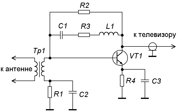
Fig. 1. Single-stage amplifier
The point of excitation of the antenna are connected directly to a balanced cross-section of the transformer TR1, which provides broadband matching of the input of the antenna to the input of the amplification stage. The amplifying element VT1 is connected to the common-emitter circuit. This allows for a greater bandpass gain and better noise properties of the scheme in comparison with other options enabled. The effects of cutoff frequency of the transistor on the steepness of the change of the gain and the input impedance in the operating frequency range is compensated for by the use in the scheme of combined frequency-dependent feedbacks parallel and serial type. Concurrent feedback is performed on the elements R3, C1, L1. Resistor R3 determines the coordination of the amplifying module in the connection joints in meter and the lower part of the UHF.
In the upper part of the operating range where the gain drops by 2-4 dB, the inductance L1 reduces the effect of this feedback, aligning the amplitude-frequency characteristic (AFC). Capacitor C1 provides decoupling the feedback circuit with the power circuit and simultaneously forms the low-frequency cutoff of the transfer characteristics of the device. Circuit R4, C3 is a consistent element current feedback, defining the main parameters of the cascade in small-signal mode: resistor R4 sets the nominal gain of the stage, and setting up C3 adjustable recovery response in the upper part of the operating range. Set parameters dynamic range enabled by selecting the type of transistor and its mode of operation. In the presented scheme the mode of operation of the cascade DC is set R4 together with the basic elements of the divider R1 and R2. Capacitor C2 bypasses R1 and provides the asymmetry connect TP1 to the schema module. Amplifier module implemented on medium power transistor of the third generation, provides a gain of 15 dB in the frequency range 40-800 MHz, the noise figure of the device does not exceed 3.5 dB and the dynamic range for television signals is 75 dB. Reduction of noise figure and implementation of most of linearity of the device when used in the schema, a complex of active elements with kaskadnym inclusion or during the transition to dvukhchastotnym the cascades.
Two schematic diagrams representing an aperiodic two-stage amplifier bipolar microwave transistors included in the circuit with the MA presented on Fig. 2.
The amplifier in Fig. 2,and contains two broadband gain stages on transistors VT1 and VT2. The signal from the actual antenna via a matching transformer (not shown) and the capacitor C1 is supplied to the base of transistor VT1, connected in the circuit with the MA.
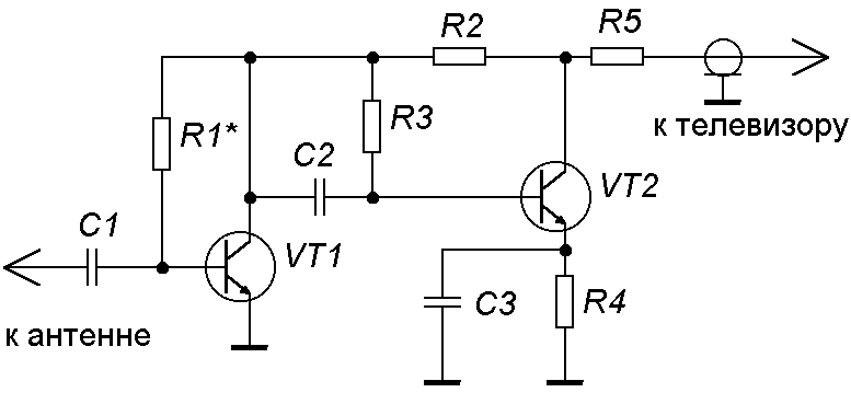
Fig. 2,and. Two-stage amplifier
The working point of the transistor is set by the bias voltage determined by the resistor R1. The current negative feedback (EP) linearizes the voltage characteristic of the first stage, stabilize the working point, but it reduces the gain. The frequency correction in the first stage is missing. The second stage also performed on the transistor on the circuit with the MA and EP voltage through resistors R2 and R3, but has a current EP via the resistor R4 in the emitter circuit, the stabilizing mode of the transistor VT2. In order to avoid large losses gain resistor R4 is shunted AC-coupled by capacitor C3, the capacitance of which is chosen relatively small (10 pF). As a result of the low frequency range of the capacitive resistance of the capacitor C3 is significant and emerging environmental AC reduces the gain, thereby correcting the frequency response of the amplifier. The disadvantages of such an amplifier circuit may include passive losses in the output circuit of the resistor R5, which is included so that it falls as a constant voltage and the signal voltage.
Similarly constructed amplifier in Fig. 2,b , which also has two cascades, collected under the scheme with the MA. It differs from the previous amplifier best isolation of power circuits using l-shaped filters L1 C6, C4 and R5 increased gain due to the presence of the capacitor C5 in the chain EP (R3 C5 R6) of the second stage and transitional capacitor C7 to the output.
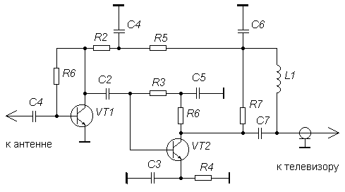
Fig. 2,b. Two-stage amplifier
In the cascade transistors connected in the circuit with the MA, the most important of the internal connections and tanks transitions of transistors. It manifests itself in limiting the bandwidth and the tendency of the amplifier to the excitation, the probability of which is greater, the higher the gain. For its evaluation it is known the concept of tolerance - limit values of gain, above which the amplifier becomes an oscillator. As a measure of sustainability can offer switch transistors on cascadei the circuit with the MA-ABOUT.
Chastnoe switch transistors VT1 and VT2 (Fig. 3) allows good forward and get most of the broadband amplifier module. This gives you the opportunity to refuse the use of signal feedbacks, stabilizing and correcting the amplitude-frequency characteristic and the input and output impedances of the link. Here the transmission coefficient and the connecting circuit parameters are set regime. To reduce the influence of parasitic inductances General conclusions, which reduce the gain of the stage at higher frequencies, the emitter conclusions input tansistor connect directly to the housing, and the mode is stabilized with a fixed base current. The high-frequency section is governed by the inductance L1 included in the collector circuit of the final transistor.
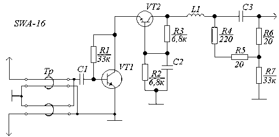
Fig. 3. Amplifier with kaskadnym enabling VT
The range correction and stabilization of the output resistance is performed by resistor-capacitor circuits. Cascada scheme is in the implementation of optimal operation of transistors allows to obtain a reduced intermodulation distortion.
In the presence of antenna VHF-UHF, structurally executed in the form of two electrically not connected antennas it is possible to use an amplifier module that amplifies the signals from each of them, summarizes and transmits to the TV receiver via a single cable. The power amplifier is fed by the same cable. Schematic diagram of the amplifying module is depicted in figure 4. It contains two independent channels of amplification. Signal MV is supplied to the contacts 1, HT, which is connected to the input stage of the channel MV harvested on transistors VT1, VT2 under the scheme of the differential amplifier. This allows us to obtain good agreement with high-impedance antennas, as well as to suppress common mode noise.
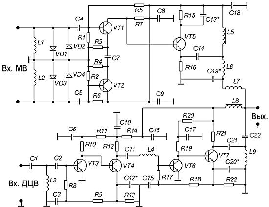
Fig. 4. Amplifier with separate entrances MV and DCV
At the entrance of the cascade set of coils L1, L2, eliminating the accumulation of static electricity charges on some antennas and diodes VD1 - VD4, protecting the amplifier from lightning. Transistor VT5 collected additional amplifying cascade. The transmission coefficient of the channel is equal to 15…20 dB. Signals MV pass the cable through the low pass filter C19 L6 L7 with a cutoff frequency of 250 MHz. Through the same filter and the throttle L5 per channel supply voltage comes from the lead-in cable. In addition, the filter does not transmit signals DCV.
Channel gain UHF consists of two series-connected similar amplification stage. The first one is assembled on transistors VT3, VT4 scheme with a galvanic connection, thereby automatically achieving the preset operation mode and maintaining that temperature and supply voltage. At the input of the cascade is set the high pass filter C1 L3 C2 with a cutoff frequency of 450 MHz, which suppresses low frequency signals and noise. Similar C21-pass filter L9 C22 at the output of the second cascade passes the UHF signals and does not transmit the signal MV. Consequently, the filters at the outputs of the channels are mutually untie them. Coil L4 provides the coordination between the stages of channel UHF and correction of the total response. The total channel gain is equal to 32…36 dB. Channel UHF powered through the inductor L8 with reduce cable. The amplifier module is powered by 12 V with current of 70 mA.
It is important to note that the modules with cascade chain structure usually provide greater linearity of the transfer characteristic, which is associated, primarily, with separate settings cascades (optimization of the transfer characteristics, modes of coordination and dynamic range) at which the thresholds of increasing overload relay and in proportion to the increase of the transmission coefficient.
Comparative analysis of technical solutions and functional-energetic characteristics of the modules shows that the underlying structures in the design of the amplifying modules for active broadband antenna advisable to choose the circuit chain with the inclusion of the cascades combined with frequency-dependent feedback. Moreover, in the first stage depth feedback is selected based on the desired value of noise figure and stability of the connecting impedance. The mode of operation and the type of transistor output stage is primarily determined by the required load capacity of the module.
Publication: www.library.espec.ws, www.cxem.net