


")

Offer to repeat the ham radio antenna amplifier UHF range (21 - 69th TV channels) has a very small size thanks use miniature chips. This was significantly different from previously discussed in the magazine.
With the development of TV broadcasting in UHF increasing interest to ham radio antennas and antenna amplifiers of this range and the availability a variety of element base allows you to develop antenna amplifiers very miniature. Typically, they perform at low noise bipolar, at least - on field-effect transistors. Currently steel is also available integrated chip, on which you can gather a subminiature low-noise antenna amplifiers UHF.
An example is a monolithic GaAs integrated circuit МGA86563, manufactured by HEWLETT-PACKARD. It is a broadband microwave amplifier with a frequency range from 0.5 to 6 GHz.
The basic parameters of the chip
- Gain (2.4 GHz), dB......21,8
- Noise figure (2.4 GHz), dB......1,6
- The voltage, V......5
- Current consumption, mA......14
Output power at compression gain by 1 dB, mW (more than 0.3 V at a load impedance of 50 Ohms) 2
Release the chip in two buildings: SOT-143 and subminiature SOТ-363. The cost of the chip in subminiature housing below and equal to several dollars. However, the performance of a uniform gain throughout range of operating frequencies of the chip (up to 6 GHz) difficult to obtain, but for antenna amplifier UHF (900 MHz) is not required.
Feature chip - receipt of the supply voltage to it via the output conclusion. This allows you to use it in the antenna amplifier supply voltage power output cable without any special circuitry.
To build on this chip low-noise antenna amplifier in common requires a minimum of parts. However, this approach, in the author's opinion, cannot considered to be correct. The fact is that, like all chips within the microwave frequency range, MGA86563 very sensitive to the charges of static electricity, overload input and excess voltage. It is typical for antenna amplifiers, it is therefore necessary to take measures to protect the device from harmful factors. The amplifier of course, a bit complex, but increase the reliability of his work.
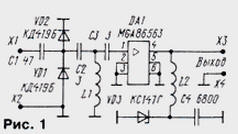
Schematic diagram of the amplifier, the author, is depicted in Fig. 1. On his entrance set the diodes VD1, VD2, which protect the chip from electrical discharges and powerful radio signals. The high pass filter С2L1C3 with cutoff frequency about 450 MHz suppresses signals with lower frequencies and thereby also protects the chip from powerful low-frequency signals. Output circuit connected directly to the output of the amplifier and cables (contacts X3, X4). To protect the output circuit from over-voltage or voltage negative polarity at the output through the inductor L2 switched capacitor C4 and the Zener diode VD3. These small complications amplifier resulted in a significant as to protect the chip from exposure to harmful factors.
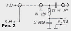
If the amplifier is planned to be placed near the antenna, it is possible to nurture it recommended through the cable drop from a stabilized power supply (9…15 V) necessarily through a current limiting resistor, as shown in Fig. 2.
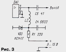
When placing the amplifier near your TV or elsewhere residential premises, the supply voltage is served in accordance with the scheme in Fig. 3.
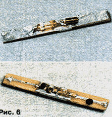
All the details of the amplifier can be placed on the PCB of bilateral foil fiberglass with a thickness of 1 mm and a size 5x(25 to 40) mm. Sketch the conductors of the circuit Board represented in Fig. 4, the placement of the elements in Fig. 5.
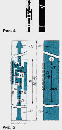
One of the sides of the Board left metallized and connected to the common wire the other side of the foil along the edge of the Board (shown by a dotted line). Most details are located on one side of the Board, and the elements L2, C4 and VD3 on the other and connected with the other through hole. The appearance of both sides of the Board shown in Fig. 6.
The amplifier can be used small capacitors, surface installation K10-17, K10-42 or similar foreign production. Coil L1 contains four coil, and L2 - 15 turns of wire sew-2 0,2 wound on the mandrel with a diameter of 1.5 mm. the Capacitors C1 - C3 is installed on the Board "lying" and C4 - "standing". The latter is soldered to the findings of the Zener diode VD3 and coil L2.
Since the size of the Board and all the elements are very small, the installation should be carried out poorly heated soldering iron, the tip of which is sharpened, and it is desirable low-melting solder. Soldering iron, Board and installer must be "grounded" for avoid chip damage by static electricity charges. If it will appear that the lower the frequency of the received interval will be above 500 MHz, should increase the number of turns of the coil L1.
After installation and test operation of the amplifier all the details for strength and protection against environmental influences is covered with a layer of epoxy glue. When using an amp outdoors it is placed in a protective housing in a plastic tube with an internal diameter of 5, an external diameter of 8 and 7… length 18…25 mm. Case with small friction wear on the Board so that it closed details. After that, the voids inside the tube gently pour epoxy glue, and then the whole amp except the places to which the solder cables, cover with a layer of water-resistant paint or varnish.
The amplifier assembled according to the scheme, and in this Board, provided the gain 19…20 dB non-uniformity of gain across the UHF range is not more than 3 dB.
Set the amp can be anywhere in the gap reduce cable antenna. When this solder points and the exposed parts of the cable must be secured to protect from oxidation and the ingress of moisture proof paint or varnish.
In conclusion, it should be noted that the scope of this chip is not limited only case considered. It can be used in a number of other designs.
Author: I. Nechaev, Kursk