


")

It has the following main technical characteristics:
Rated output power....... 75 watts
THD.......... 0,06%
The bandwidth of.......... 20 … 40 000 Hz
The signal-to-noise.......... 86 dB
The voltage........... ±40 In
Quiescent current.............. 20 mA
The improvement of quality indicators in this amplifier compared to the previous achieved near circuit design. In the emitter circuit of the input differential stage includes the current source FET. This improves the transmission coefficient of the first stage and to improve its thermal stability. To improve the symmetry of the shoulders of the output stage of the amplifier and reduce the nonlinear distortion in the emitter circuit of one of the transistors predominance cascade introduces a correcting circuit consisting of a diode, resistor and capacitor.
Schematic diagram of the amplifier shown in figure 1. It contains a differential input stage (VT2, VT4), a current amplifier (VT3) and voltage {VT6) output stage (VT9-VT12) and a protection against overloads (VT7, VT8). As already mentioned, the current source transistor VT1 included in the emitter circuit of transistor VT2, VT4, allows, without increasing temperature instability, increase the gain of the voltage differential stage. The transistor VT3 allows you to reduce the load on the output of the differential stage. Cascade split load transistor VT6 amplifies the voltage signal, providing a maximum output voltage swing.
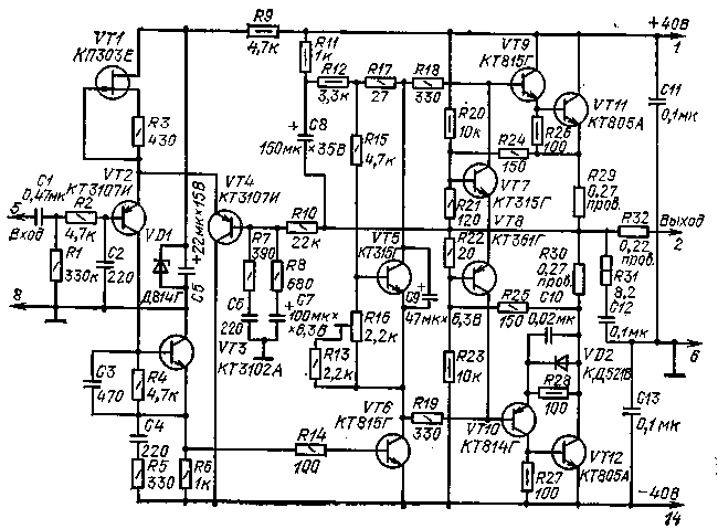
Figure 1
Quasihereditary output stage, is based on the composite transistors (VT9, VT11 and VT10, VT12), fits well with the low-impedance load. Correcting circuit consisting of a parallel connected diode VD2, resistor R28 and capacitor C10, improves the symmetry of the shoulders of the amplifier, thereby reducing harmonic distortion. The initial offset at the bases of the output transistors to work in AV mode is determined by the voltage drop on the section of the collector-emitter of the transistor VT5 and regulated by the resistor R16. The transistor VT7 and VT8 shunt overload emitter junction of the output transistors, thereby effecting their protection. Elements C3, R5, C4, R31, C12 prevent self-excitation of the amplifier at high frequencies. The circuit R7, Sa is used to equalize the frequency response of the amplifier at high frequencies of the audio range (20 kHz).
Structurally, the amplifier is assembled on the circuit Board. Temperature stabilization of the quiescent current of the output transistors by using the transistor VT5 installed in common with VT12 VT11 or the radiator; in the immediate vicinity. For power amplifier bipolar required source supplying voltage ±40 V current is not less than 2.5 A.
The establishment of an amplifier, harvested from the healthy elements, is to verify the correct installation of the quiescent current of the output transistors resistor R16 in the range of 20 to 40 mA.
Literature
D. I. Atayev, V. A. Bolotnikov. Practical schemes of high-quality sound reproduction. M. Radio and communications. 1986.