


")

The amplifier has the following specifications:
Rated output power....... 55 W
THD.......... 0,07%
The bandwidth of.......... 20… 50 000 Hz
The signal-to-noise...............89 dB
The voltage........... ±36 In
Quiescent current.......... 100 mA
One of the features of this amplifier is its power from bipolar source. This allows you to include the load between the outputs of the amplifier and the common wire without transition capacitor. Another feature is the use of balanced input differential stage having a good thermal stability.
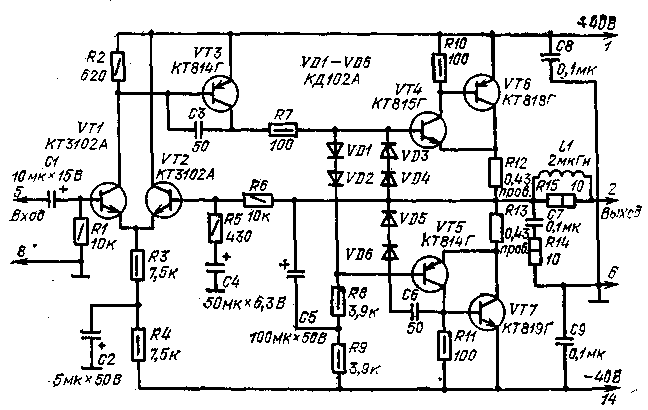
Figure 1
Schematic diagram of the amplifier shown in figure 1. It consists of an input stage (transistors VT1. VT2}, cascade voltage gain (VT3), output (VT4-VT7), elements of protection of the output transistors (VD3-VD6). The input stage is the scheme of the differential stage single-ended output. The input signal is supplied to the base of transistor VT1 through the coupling capacitor C1. The signal EP is supplied from the output through a resistor R6 to the 'base of transistor VT2. A differential stage compares the output voltage with zero voltage common wire, and if for any reason the DC voltage at the amplifier's output will be different from zero, the error signal from the output of the differential stage is fed to the output stage, thereby providing a zero voltage at the amplifier output. From the output of the differential stage, the signal is sent to the amplifier and through a resistor D7 at the output stage. The output stage is based on the composite of complementary transistors VT4, VT6 and VT5, VT7, with extensive input and very low output impedance.
Diodes VD1 and VD2 create an initial offset of the output stage and provide temperature stabilization of the quiescent current of the output transistors. Through the condenser valittomasti C5 connects the PIC on target. the collector load of the transistor VT3, thereby obtaining the maximum time-
Maha output voltage. Diodes VD3, VD4 and VD5, VD6 protect the output transistors, continue in case of overload, the transitions of transistors. Elements NW, C6, R. 14, C7, L1 prevent self-excitation of the amplifier at high frequencies.
For temperature stabilization of the quiescent current of the output transistors diodes VD1 and VD2 is set in common with the transistor VT6 VT7 the heat sink. Coil L1 is wound on the resistor R15 (MLT-2) and contains 25 turns of wire sew-2 to 0.8. Resistors R12 and R13 are made of high resistance wire (manganin, Constantan).
The establishment of an amplifier is to verify the correctness of the installation. With proper installation and use of the healthy elements additional configuration is required. For power amplifier bipolar required source supplying at a voltage of ±36 V current is not less than 1.2 A.
Literature
D. I. Atayev, V. A. Bolotnikov. Practical schemes of high-quality sound reproduction. M. Radio and communications. 1986.