


")

Relay, the circuit of which is shown in Fig. 1, is intended to enable and disconnect the rear fog lights in accordance with the algorithm rule No. 048 UNECE.
Switching on the rear fog lights by single clicking on the closing button, connected between pin 3 ("General") and 5 ("On/off") in the presence of the supply voltage to pin 2 ("Fog") and/or 6 ("Low beam/high beam") connector X1 (i.e. included if the lights dim or a headlight and/or fog).
Off rear fog lights by single clicking on the same button or when you remove the voltage at pins 2 and 6, and in the case of re-supply voltage on pins 2 and/or 6 rear fog lights are not included.
Today, different companies have begun production of three modifications relay: 23.3777 - on the basis of the D-flip-flop collected transistors; on the chip KTM; 22.3777 - on chips KIT.
Each modification has its advantages and disadvantages. The main advantage rule first two options - the simplicity, small number of parts and low cost. The main drawback of the first relay - low temperature stability due to the use of transistors in the D-flip-flop. This disadvantage is not present in a second embodiment of the relay, however, the presence of the sloping front of the signal may result in the through current IC, which, in turn, long-term operation the product is the cause of the release and, accordingly, only the relay down.
The main advantage of the third option of the relay - steep fronts of governors signals due to the use of a Schmitt trigger, which eliminates the occurrence of through current and thereby results in a high stability of the device in General. The main disadvantage is the complexity, a large number of elements and their the high cost.
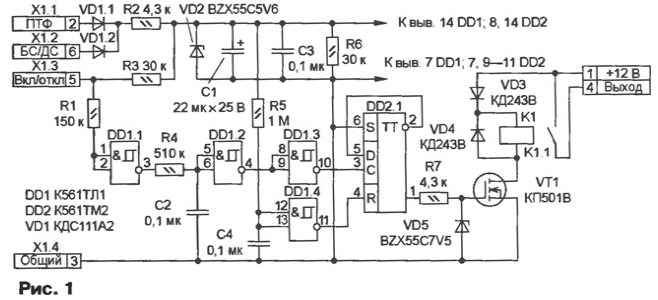
Consider a third option relay in more detail. The device consists of the following functional units: the node power (VD1 diode, Zener diode VD2, resistors R2, R6, capacitors C1, C3); a driver control signal (Schmitt triggers DD1.1 - DD1.3, resistors R1, R3, R4, capacitor C2); the initial node setup (element DD1.4, resistor R5, capacitor C4); trigger (element DD2.1); switch (the transistor VT1, diodes VD3, VD4, the Zener diode VD5, the relay K1, the resistor R7).
The node power - parametric voltage regulator that provides the necessary nourishment and protection relays.
Driver control signal performs the function of protection from unstable enable/disable the relay due to contact bounce of a button and from spontaneous enable/disable relay due to interference in the management chain.
The initial node setup provides off-state relay when submitting the voltage on the node power.
Trigger implements the desired algorithm of the device.
The switch is made on electromagnetic relay K1, which is controlled transistor VT1, delivers the power to the rear fog lights.
When voltage is supplied to the contacts 1 and 2 and/or 6 of connector X1, all the relay nodes get power, but the switch is off, the contacts K1.1 relay K1 open. If one of these contacts connector voltage disappears, the relay will shut off already rear fog lights.
When you press the button connected to the pins 5 and 3 of connector X1, trigger changes its state, the switch is triggered and turns on the rear fog lights. If you double click the button, a switch, and, accordingly, rear fog lights will turn off.
Time diagram of the relay shown in Fig. 2. Here tп - the time of filing the supply voltage.
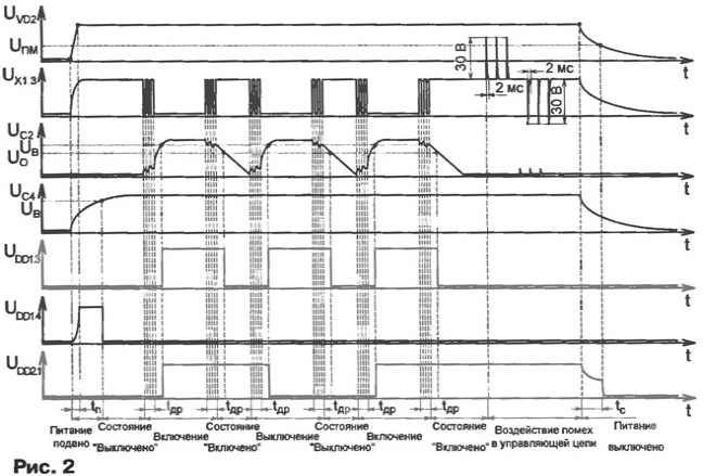
Estimated value of 50…60 MS, is determined by the resistance of the resistor R2 and the capacitance of the capacitor C1; tc is the time of removal of the voltage. Approximate value - 0,5…1, is determined by the resistance of the resistor R6 and the capacitance of the capacitor C1; tдр - time contact bounce button connected between pins 5 and 3 of connector X1. The estimated value of 20…30 MS; IPM - the minimum supply voltage of the chip CTL and CTM. Approximate value - 2…3 V; UB - switching voltage of the Schmitt trigger circuits CTL. The estimated value is 3.6 - 3.8 V; Uo - off voltage Schmitt trigger circuits CTL. Approximate value - 1,9 1,8… V.
The device incorporates components of both bulk and surface (resistors and capacitors, with the exception of oxide) of the installation. Resistors and ceramic capacitors - sizes 1206, the oxide capacitor (C1) - aluminum production company HITANO [1]. Against polarity reversal power source and powerful electromagnetic interference relay protects the high-voltage diode Assembly CDSA (VD1) and the diode KDV (VD3).
Field-effect transistor KW (VT1) of the voltage of self-induction when switching relay coil K1 (91.3747 - 10 production of "AVAR", Pskov) protected high voltage diode KDV (VD4). Chip DD1, DD2 series C [2] eat from parametric stabilizer on the Zener BZX55C5V6 (VD2) PHILIPS [3]. Zener BZX55C7V5 (VD5) PHILIPS protects direct access to the trigger DD2.1 from surges, "penetration" through the capacitance drain-gate transistor VT1.
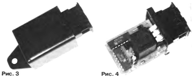
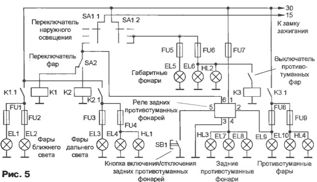
Relay (Fig. 3) consists of a housing, a circuit Board (Fig. 4), where assembled all the elements, and the six pin connector to connect the product to the vehicle network (Fig. 5).
PCB bilateral, on one side placed elements for surface mounting, on the other - all the rest of them.
Literature
Author: D. Matveev, Cheboksary