


")

This device provides continuous radio status monitoring protected object. If any unauthorized impact on him or the failure of the transmitter, the receiver will immediately inform the owner an alarming signal.
This device provides continuous radio status monitoring protected object. If any unauthorized impact on him or the failure of the transmitter, the receiver will immediately inform the owner an alarming signal.
The radio channel is described by a guard device consists of a transmitter, installed in the vehicle, and a receiver held by the owner. In standby mode transmitter with every 16 emits a frequency modulated on the parcel frequency 26945 kHz (the choice of radio channel parameters can be found from [1]). The duration of the parcel - 1 S. modulation frequency of 1024 Hz. When triggered alarm sensors, the transmitter switches to a continuous modulated radiation, on which the receiver will respond alarming. The same signal will sound if the receiver is not received another parcel through 16 after the start previous.
This algorithm radiostacja provides high reliability protection, since any defect - curse of the antenna, the battery is discharged or exit building the transmitter is immediately marked with a warning signal.
Transmitter output power is 2 W, receiver sensitivity is better than 1 mV. With compact transmitter antenna mounted behind the windshield car, and pin receiver antenna length of about 50 cm range radio channel exceeds 500 m. If the car and in the receive location to use full-size antenna, the range may reach several kilometers.
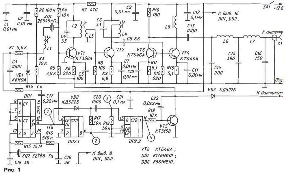
Diagram of the transmitter of the guard is represented in Fig. 1. On chips DD1 and DD2 assembled hub, providing the necessary temporal rhythm of his work. Specifies generator chips DDI stable "hour" quartz resonator ZQ2. The output signal F of the counter circuits DD1 [2] generator modulates the transmitter, and from the output of S1 is input to the CN counter DD2.1 and diode-capacitor switch VD2R17C20R18.
(click to enlarge)
While the output counter in DD2.1 a logic low pulses with a frequency of 1 Hz pass through the switch and reset the counter DD2.2 (Fig. 2. of the market. 2 and 3). When the counter output 8 DD2.1 a logic high is closed diode VD2 and the pulses at the input R of the counter DD2.2 cease to act. At the moment the appearance of negative differential input CP of the counter DD2.2 he goes into one state and at its output 1 appears high logic level.
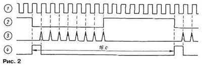
The next pulse from the output S1 of the counter DD1. passing through the opened diode VD1. resets counter DD2.2. Thus, the counter DD2.2 generates the output 1 the high level pulses with a duration of 1 s with a repetition period of 16 s (Fig. 4).
The high level pulses from the output of the counter DD2.2 open commuting the transistor VT5, allowing the operation of the generator carrier transmitter. The basis the transmitter of the device is taken, are described in the brochure [3]. The generator is assembled on transistor VT1 and stable quartz resonator ZQ1. The modulating signal with a frequency of 1024 Hz is applied to the varicap VD1. Modulation narrowband. The deviation in a small change within the podstroechnik coil L1.
Fluctuations of the operating frequency of the generator emits an oscillating circuit L2C4. Through coupling coil L3 signal is input to the buffer resonance amplifier the transistor VT2 mode S. the Load transistor circuit is L4C6. Through the capacitor C8 amplified signal supplied to the input of the power amplifier, which is made of two parallel connected transistors VT3 and VT4. also operating in mode S. the Output signal of the amplifier through the coupling the capacitor C13. the filter C14 L6 C15 L7 C16 and connector X1 is supplied to the transmission the antenna or cable with a characteristic impedance of 50 Ohms.
The transmitter goes into a continuous emission mode when actuated, security sensors, closing the cathode of the diode VD3 to the vehicle body. If necessary unleash the sensors should be installed several of these diodes, the anode which is connected to the collector of the transistor VT5. If any of the sensors in the response form the high signal, the output of each of them connected to the base of the transistor VT5 through the series-connected resistor resistance 20…33 ohms and any low-power silicon diode (cathode to base).
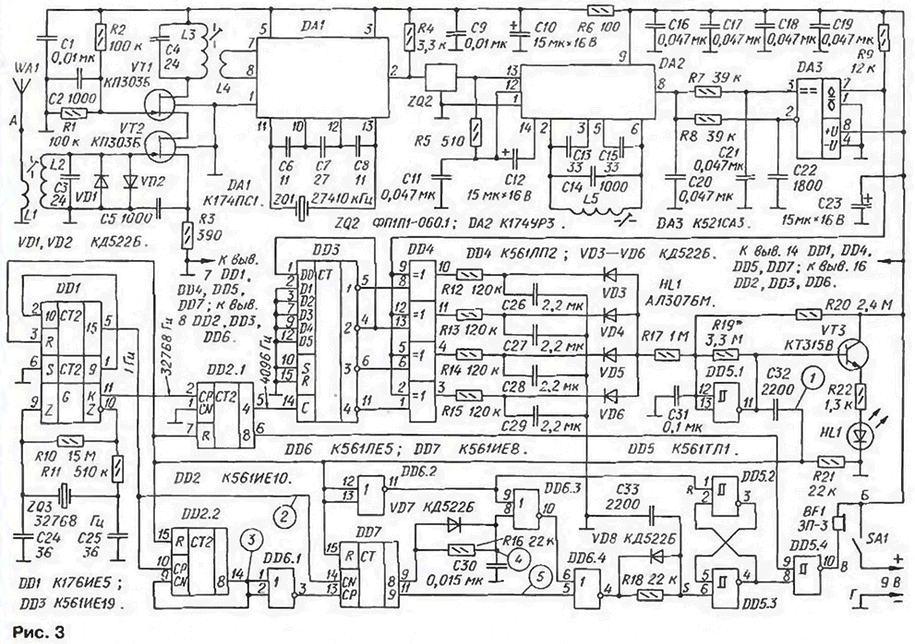
The receiver circuit of Radiolaria depicted in Fig. 3. The high-frequency part assembled according to the traditional scheme. The adopted antenna WA1 signal is input circuit L2C3. Diodes VD1 and VD2 are used to protect the input of the RF amplifier when the amplitude of of the input signal. The RF amplifier is assembled by kaskadnoi scheme on field-effect transistors VT1 and VT2. The load of the amplifier circuit is L3C4.
(click to enlarge)
The mixer is made on the chip DA1. She also performs the functions of the local oscillator, the frequency of which is stabilized by a quartz resonator ZQ1. The frequency of the resonator can be more or less than the frequency of the transmitter at 465 kHz. i.e. either 26480. either 27410 kHz. With the load of the mixer, resistor R4, the if signal is supplied to piezoelectric ceramic if filter ZQ2. providing the required selectivity receiver. Chip DA2 performs signal amplification, restriction and frequency detection. Resonant circuit C14L5 frequency detector configured the frequency of 465 kHz.
The demodulated signal frequency of 1024 Hz is supplied to the inputs of the comparator DA3 in two of the integrating circuit, wherein the value of the time constant. On direct entry signal is sent through a chain R7C21. almost completely overwhelming useful signal and the inverse signal comes through the chain R8C22 almost without loosening.
This node is a bandpass filter. At a frequency of 1024 Hz it forms the output sequence of pulses, in the form close to "meander" and the input signals with a frequency substantially different from 1024 Hz. the output is practically not pass.
From the output of the comparator DA3 signal is input to the digital hub. The rhythm of his work sets the generator on the chip DDI. the frequency of which is stabilized same. as in the transmitter, a quartz resonator for a frequency of 32768 Hz. Weekend the pulse generator with a frequency of 32768 Hz output To arrive at the input CP of the counter DD2.1 control channel frequency, and a frequency of 1 Hz From the output 15 of the counter chip DDI to the input CP of the counter DD2.2 and the input of the CN counter DD7 channel control time intervals.
DD2 counter.1 generates pulses with a duty cycle 2. Counter DD3 - five digit a shift register that, when combined output 2 to input D0 divides the frequency the four pulses [4]. The outputs 1 to 4, it generates a signal of the form meander with a phase shift of 0, 90, 180 and 270°.
These four signals arrive at the bottom on the inputs of the circuit elements DD4.1 - DD4.4, and upper inputs connected together filed an output signal of the comparator DA3. When the absence of an input signal at the output of the comparator operates noise voltage. After mixing in elements DD4.1 - DD4.4 with the output signals of the counter DD3 noise averaged integrating circuit R12C26. R13C27. R14C28. R15C29. As a result, the voltage on the capacitors C26 - s't care about half of the supply voltage. At the input of the Schmitt trigger DD5.1 taking the fall on the diodes VD3 - VD6 and the resistor R17 voltage exceeds the upper switching threshold trigger, so its output will be a logic low.
When the output of the comparator voltage with a frequency of 1024 Hz is the multiplication of elements DD4.1 - DD4.4 with the output signals of the counter DD3. If the inputs of any of these elements, the phase of the signals are the same, at its output will be low, when the anti-phase signal is high, and at similar phases - pulses of high duty cycle, and the average voltage of these pulses is close to zero.
So after about 0.5 s after the start of the reception of the desired signal is one of capacitors C26 - s corresponding to that element chip DD4. phase the input signals of which the closest is discharged to nearly zero. The input voltage of the Schmitt trigger DD5.1 is below the lower threshold switch and its output goes high level.
After about 0.5 s after the end of the reception of the desired signal on the capacitors C26 - s again sets the voltage close to half of the voltage power, and the Schmitt trigger DD5.1 passes to its original state. Thus, at its output pulses of high-level duration approximately corresponding input and delayed relatively to 0.5 S. HL1 Led flashes at 1 to indicate the presence of a useful signal in the antenna WA1. Negative OS through a resistor R19 slightly reduces the width of the loop "hysteresis of Schmitt trigger. Bandwidth mentioned above a kind of filter is about 2 Hz, and the modulation frequency outside 1023 1025… Hz Schmitt trigger DD5.1 won't work.
Will see how it acts after the activation of the host digital processing when receiving signal parcels with a frequency of 1024 Hz and a repetition period of 16 with the Chain C32R21 differentiates the edge pulse is generated at the output of the element DD5.1. A short pulse of positive polarity - we will call it control (Fig. 1 in Fig. 4) is fed to the input R of the counters DDI. DD2.1. DD2.2. DD7. and also through inverter DD6.2 input R of flip-flop collected on elements DD5.2 and DD5.3. translating the trigger is in the zero state. This short pulse passes also through the elements DD6.3 and DD6.4 with a low level at the outputs 8 and 9 of the counter DD7 and at input S sets the trigger DD5.2. DD5.3 in one state, when which the output element DD5.3 high logic level.
The pulse received at the input S of a flip-flop has a duration greater. than the input R of the action of the circuit R18VD8C33. therefore, after the falling pulse trigger remains in a single state holding element DD5.4 open. Because upper circuit on the input of this element from the output 8 of the counter DD2.1 do the pulses of the square wave with a frequency of 2048 Hz. sounds a continuous tone. Pulses with a frequency of 1 Hz is received from the output 15 of the counter DD1 to the input CP of the counter DD2.2 and CN - DD7 (Fig. 2). Then, the first of them considers these impulses by their decay, second blocked high level input CP from the output of the inverter DD6.1.
After 8 with the output 8 of the counter DD2.2, there is a high level (Fig. 3). He stops and samolocie counter DD2.2. To recover from this state the counter only after the course to its input R reset pulse. The signal output from counter DD2.2 after inverting element DD6.1 enables the counter DD7, counting the seconds pulses on their front. Even after 7.5 with the output 8 this counter appears high level.
Thus, after a 15.5 with after the appearance of a control pulse at the lower circuit on the input of the DD6.3 there is a high level, kept in for 1 s (Fig. 4). if you do not change the mode of the counter inputs DD7.
When a new control pulse (after 16 seconds after the previous one) he switches to the zero state trigger DD5.2. DD5.3 and the audio signal ceases. The pulse does not pass through the elements DD6.3, DD6.4. because the lower input of the DD6.3 high level.
In the time of arrival of the control pulse counters, including DD7. reset; however, on the lower input of the DD6.3 due to the action of the chain VD7R16C30 change high low level is delayed by approximately 200 μs. It guarantees the prohibition of passing a short test pulse (the duration about 30 μs) to the input S of the flip-flop DD5.2. DD5.3. Therefore, when you receive the control pulses of the trigger remains in the zero state and the alarm sounds. The described process is illustrated in Fig. 4 in solid lines.
If the next control pulse through 16±0.5 s is not received, the work the device will occur. as shown in Fig. 4 by dashed lines. A high level. appeared later 16.5 with the output of counter 9 DD7. install the trigger DD5.2. DD5.3 in one state and the bell will ring. It'll stop only when the receiver comes two pulse at an interval of 16 C.
The alarm will also sound if the impulse occurs quicker 15.5 with after previous, since there will be no ban on the output side 8 of the counter DD7 on his passing through the element DD6.3.
Thus, the systematic arrival of the signals with a modulation frequency of 1024 Hz and period of 16 since the system is in standby mode, the led HL1 on it the front panel flashes to indicate that the serviceability of Radiolaria in General and the passage of radio signals. Any deviation from the specified rhythm begins to sound the alarm. Continuous illumination of the led HL1 actuation means any security sensor, and the absence of light - discontinuance of the transmitter or the deterioration of the radio below the acceptable level.
The transmitter is assembled on PCB from bilateral foiled fiberglass thickness 1.5 mm the Drawing Board is presented in Fig. 5. On the component side foil saved and serves as a common wire. The findings are soldered to GND without holes. For the remaining conclusions are drilled through holes and the common wire razzenkovannoe. All soldering points to a common wire is marked in the drawing crosses. The holes for the "grounding" the leads of the chips do not need to countersink.
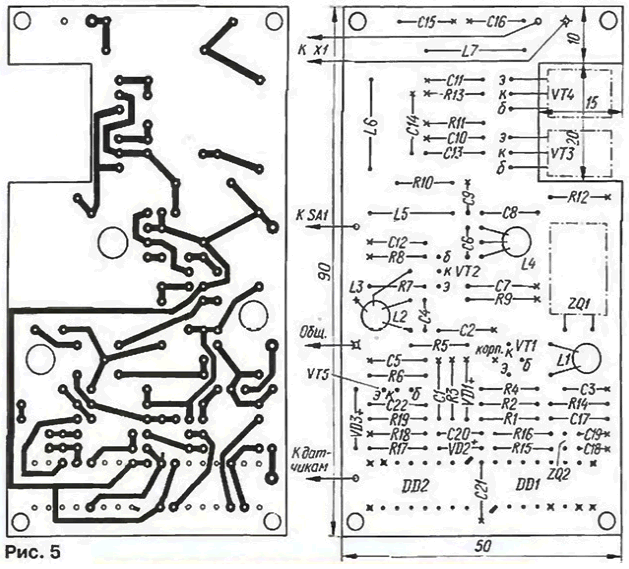
At the points of connection of the Board with an antenna connector X1, power supply and sensors in the holes and pressed opaânnymi tin pins with a diameter of 1 mm as pins it is convenient to use the contacts from the connector RM.
Transistors VT3 and VT4 are soldered to the printed conductors, findings need pre-bend at right angles. During final Assembly of the transmitter transistors screwed to the metal casing of the device, serving to them the heat sink. Exclude them from the casing of thin mica spacers.
The transmitter used resistors MT and MLT, capacitors km-5 km-6. Transistor CTV can be replaced by any low-power silicon structure of the n-p-n, and the transistor CTA - any of the series CT, CT. Instead CTA suitable the series transistors CT and CT, but will have to overcome the complexity of abduction heat.
Diodes VD2 and VD3 - any silicon thin. The varicap LW110A to replace LW109, LW124, D with any letter index. Quartz resonator ZQ1 - standard, metal flattened body, a ZQ2 - in miniature cylindrical housing, from watches.
Coil L1 L2L3 L4 and is wound round three polystyrene frame with a diameter of 5 mm. trimmers equipped with carbonyl iron. Coil L1 contains 25 turns of wire sew-2 0.25. coils L2, L4 - 12 turns, a L3 - 3 turns of the same wire. The coil L3 is wound on top L2. a L4 has an outlet from third from the top of the loop scheme.
The inductor L5 is wound on the ring size K10h6h3 ferrite NN. Winding contains 15 turns of wire sew-2 0,15. Coils L6 and L7 - frameless wound turn to turn on the mandrel with a diameter of 8 mm and contain 5 and 9 turns of wire sew-2 0,8 respectively.
The transmitter is mounted in a metal box the size of 110x60x45 In mm. the walls of the housing has a power switch (SA1), high frequency connector SR-50-FV (X1) and the four-pin connector RM (Fig. 1, not shown) for connect the power source and the sensors.
The electrical circuit of a compact helical antenna whip normal radiation [3]. designed to work together with the transmitter shown in Fig. 6,and its design - in Fig. 6,b. On the housing of the cable connector pads SR-50-FV strengthen small plastic box (its size is not critical), which is set LC-circuit. consisting of coil L1 and trimmer the C1 capacitor with an air dielectric.
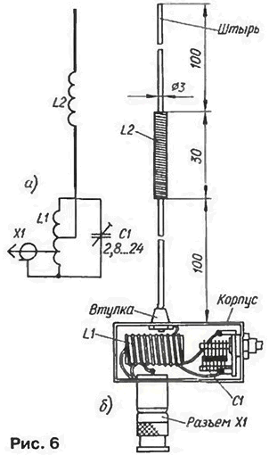
Coil L1 is wound with a pitch of 2 mm silver plated copper wire with a diameter of 1 mm on the ceramic frame with a diameter of 10 mm, Number of turns - 15. Space bends determine if adjustment of the system. The capacitor C1 is KVM.
An extension coil L2 is wound round the frame with a diameter of 6 mm from organic glass. It contains 130 turns of wire sew-2 0.15. At the ends the frame is fixed on thread two brass pins. The lower end of the bottom drawing pin screwed into the hole of the brass bushing mounted on the upper wall the plastic box.
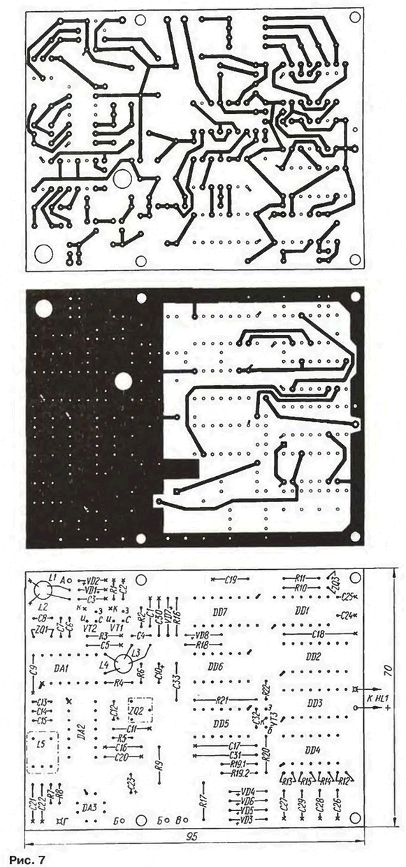
The receiver is assembled on a printed circuit Board from bilateral foil fiberglass 1.5 mm the Drawing Board shown in Fig. 7. In the same way. as the Board of the transmitter, under the elements of the high-frequency receiver foil saved and plays the role of a common wire. Saved and plastic frame around digital node. To connect the Board with the antenna, the sound projector BF1 and connector the power source in the same way as in the transmitter is pressed and opaânnymi the contact pins with a diameter of 1 mm.
(click to enlarge)
You should pay attention that the number of mounting points of the Board relating to digital node, you need to solder to both sides. At two points - they have the drawing is not round, but square - must be pre-inserted into hole a short wire jumper.
In the receiver are used resistors MT and MLT; oxide capacitors - K53-19. the rest - km-5 km-6. You can use parts of other types. Transistors KSSB can be replaced by a single dual gate. for example, CPB. Diodes VD1 and VD2 - any silicon high frequency or pulse, and the rest of silicon low-power. Instead PPP 1-060.1 and other suitable piezophilic at this frequency, having a bandwidth of at least 3 kHz, for example. PPP-60. PPP-61. Quartz the resonator ZQ3 - miniature, in the cylindrical housing.
Coil L1L2 and L3L4 wound on two identical polystyrene frame 5 mm in diameter, equipped with trimmers carbonyl iron. Coils L2 and L3 contain 18 turns of wire sew-2 0.33. winding turn to turn. Coil links L1 and L4 - 3 coils of wire PAVLO 0,2 - wound on top of their contour from the grounded output coil L2 and the output of the coil L3, connected to the positive power wire. Coil L5 used industrial manufacturing inductance 120 µh with podstroechnik. Independently it can to reel in an armored magnetic core SB-9a. the number of turns - 80. wire - sew-2 0.1.
Card installed in a plastic case from a pocket receiver dimensions 140x80x40 mm Antenna - telescopic length of about 50 cm To power the receiver used a remote network unit with an output voltage of 12 V, supplemented by the voltage regulator on a chip CREE and weekends oxide capacitor 10 µf for a voltage not less than 16 V. For reduce multiplicative noise both output secondary winding network the transformer unit is connected to its output minus the wire through ceramic capacitors of 0.1 μf. For the battery of the receiver can be applied 7D battery-0.115-U1.1.
To build and develop the system in a certain order. First and the transmitter and in the receiver gather the digital part, but without a resistor R17 in the receiver and the transmitter are installed resistors R4. R5 and R7. Connect the supply circuit of the transmitter and receiver, the collector of transistor VT5 the transmitter is connected to the inputs of the element DD5.1 receiver.
When the power supply may be included or may not be included sound the signal, however, with the arrival of the first pulse transmitter needs for a short time flashing led HL1 and start singing (or continue to sound) signal. Through 16 with HL1 led should flash again, and the signal - to stop. Further the led should turn on 1 with every 16 C. and the audio signal to remain off.
Then, in the pause between the pulses should be short circuit the capacitor C31 of the receiver that will simulate the transition of a transmitter in a continuous mode. Have sound signal. To disconnect the capacitor C31 and make sure that after passing the two pulses from the transmitter (this is well illustrated by the led flashes HL1) the beep stops. To disable the inputs of the element DD5.1 receiver from the collector of the transistor VT5 transmitter - not later than 15 must again sound signal.
Next, install the transmitter resistors R1 - R3. R14, and in the receiver - R7 - R9, R17, capacitors C21, C22 and comparator DA3. In a common point of the resistors R7 and R8 receiver via the button served from a common point of resistors R2 and R3 transmitter pulses with a frequency of 1024 Hz. When closing and opening of the contacts button should accordingly on and off the led HL1 with a slight delay (it must be visible to the eye).
If the nodes do not operate as described, the problem is how usually, when creating a digital device - check the operation of kartsovnik generators, the accuracy of frequency division in the counters and the formation of the corresponding signals etc If the manipulation button pulse the signal frequency of 1024 Hz, the led does not turn on, choose a resistor R19 I. perhaps R20. For fine selections of resistor R19 he divided into two part (and on the Board for them provides space), which is correlated to resistance as of 9:1.
After complete Assembly of the device configuration of the radio should start with of the transmitter. Temporary jumper connect the emitter and collector of transistor VT5, and as an equivalent antenna transmitter output load resistor the resistance of 51 Ohms power of 2 watts. At the time of tuning transistors VT3 and VT4 must be installed on dural plate or copper heat sink dimensions not less than 100x60 mm
Filing for transmitter power supply voltage and rotating podstroechnik coil L2, achieve generation. At the base of transistor VT2 must be present HF voltage of 0.6 V. It is measured broadband or high frequency oscilloscope with a voltmeter. The buffer stage transistor VT2 set rotation the podstroechnik coil L4 to obtain the maximum amplitude at the collector transistor VT2 (at least 5 In). Thus on the basis of transistors VT3 and VT4 should to be a voltage of less than 2 V. Dilating and constricting coils of the coils L6 and L7, to achieve the maximum voltage on the dummy - 10… 12 V. Setting transmitter clarify in the same order after it is installed in the housing.
Then configure the transmitting antenna. In the middle of the metal plate (can use and coated fibreglass) dimensions not less than 250x250 mm set the socket connector SR-50-TV and connect it with the output of the transmitter the cable, which the antenna will be connected to it by car. Set the antenna pin part of the connector in the socket and turn the transmitter on the work in continuous mode. Control of the maximum measurement lead indicator the field strength. You can use a simple wavemeter [5] by connecting to it the output of the small-sized microammeter.
Circuit L1C1 antenna tune in resonance to the maximum readings. Further choose the location of the outlet from the coil to the side of the transmitter (2…3 turns) and in side pin (6… 10 turns), also achieving the highest field strength. After installing the antenna in the car tuning circuit L1C1 specify.
For adjustment of the receiver, it is desirable to use broadband the oscilloscope. First if amplifier. A signal frequency of 465 kHz deviation of 3 kHz at the input of the circuit DA2 (pin. 13) and adjust the contour L5C14 rotation of podstroechnik coil L5 to obtain the best and Squareness pulse ratio equal to two, the output circuits DA2. If the detected excitation circuits DA2, the coil L5 should shall be shorted a low-power resistor 5 ..10 kOhm.
Then check the operation of the oscillator. If necessary, choose capacitors C6 - C8 to obtain stable generation of the third mechanical harmonica quartz resonator Z01.
Next, check the voltage at the source of transistor VT2. it should be within 0,3…0,5 V. signaled with an operating frequency at the receiver input, the rotation the trimmers coils contours L2C3 and L3C4 set up the circuits in resonance, focusing on maximizing the sensitivity of the receiver (about 0.5 mV).
In the absence of a signal generator it is possible to replace a transmitter configured without the antenna and put it to the above-mentioned resistor 51 Ohm. Have a first transmitter next to the receiver, and at least alienate settings the transmitter at the maximum distance, controlling the reception signal the oscilloscope connected to the output circuits DA2, or by the LEDs HL1.
The transmitter is quite economical - a fully charged automotive the battery capacity of 55 Ah And will last for three months continuous work in standby mode.
The described radiozero has more than three years and has already helped to prevent intruders in the car.
A lot of useful information on building a radio patrol car the various design options of antennas of the transmitter and the receiver is contained in the publications [1,6 - 8].
The transmitter is assembled on a printed circuit Board from bilateral foil fiberglass 1.5 mm Drawing card is presented in Fig. 5. By components of the foil is retained and serves as a common wire. The findings are soldered to GND no holes. For the remaining conclusions are drilled through the holes and the common wire razzenkovannoe. All soldering points to a common the wire is marked in the drawing crosses. The holes for the "grounding" conclusions chips do not need to countersink.
At the points of connection of the Board with an antenna connector X1, power supply and sensors in the holes and pressed opaânnymi tin pins with a diameter of 1 mm as pins it is convenient to use the contacts from the connector RM.
Transistors VT3 and VT4 are soldered to the printed conductors, findings need pre-bend at right angles. During final Assembly of the transmitter transistors screwed to the metal casing of the device, serving to them the heat sink. Exclude them from the casing of thin mica spacers.
The transmitter used resistors MT and MLT, capacitors km-5 km-6. Transistor CTV can be replaced by any low-power silicon structure of the n-p-n, and the transistor CTA - any of the series CT, CT. Instead CTA suitable the series transistors CT and CT, but will have to overcome the complexity of abduction heat.
Diodes VD2 and VD3 - any silicon thin. The varicap LW110A to replace LW109, LW124, D with any letter index. Quartz resonator ZQ1 - standard, metal flattened body, a ZQ2 - in miniature cylindrical housing, from watches.
Coil L1 L2L3 L4 and is wound round three polystyrene frame with a diameter of 5 mm. trimmers equipped with carbonyl iron. Coil L1 contains 25 turns of wire sew-2 0.25. coils L2, L4 - 12 turns, a L3 - 3 turns of the same wire. The coil L3 is wound on top L2. a L4 has an outlet from third from the top of the loop scheme.
The inductor L5 is wound on the ring size K10h6h3 ferrite NN. Winding contains 15 turns of wire sew-2 0,15. Coils L6 and L7 - frameless wound turn to turn on the mandrel with a diameter of 8 mm and contain 5 and 9 turns of wire sew-2 0,8 respectively.
The transmitter is mounted in a metal box the size of 110x60x45 In mm. the walls of the housing has a power switch (SA1), high frequency connector SR-50-FV (X1) and the four-pin connector RM (Fig. 1, not shown) for connect the power source and the sensors.
The electrical circuit of a compact helical antenna whip normal radiation [3]. designed to work together with the transmitter shown in Fig. 6,and its design - in Fig. 6,b. On the housing of the cable connector pads SR-50-FV strengthen small plastic box (its size is not critical), which is set LC-circuit. consisting of coil L1 and trimmer the C1 capacitor with an air dielectric.
Coil L1 is wound with a pitch of 2 mm silver plated copper wire with a diameter of 1 mm on the ceramic frame with a diameter of 10 mm, Number of turns - 15. Space bends determine if adjustment of the system. The capacitor C1 is KVM.
An extension coil L2 is wound round the frame with a diameter of 6 mm from organic glass. It contains 130 turns of wire sew-2 0.15. At the ends the frame is fixed on thread two brass pins. The lower end of the bottom drawing pin screwed into the hole of the brass bushing mounted on the upper wall the plastic box.
The receiver is assembled on a printed circuit Board from bilateral foil fiberglass 1.5 mm the Drawing Board shown in Fig. 7. In the same way. as the Board of the transmitter, under the elements of the high-frequency receiver foil saved and plays the role of a common wire. Saved and plastic frame around digital node. To connect the Board with the antenna, the sound projector BF1 and connector the power source in the same way as in the transmitter is pressed and opaânnymi the contact pins with a diameter of 1 mm.
You should pay attention that the number of mounting points of the Board relating to digital node, you need to solder to both sides. At two points - they have the drawing is not round, but square - must be pre-inserted into hole a short wire jumper.
In the receiver are used resistors MT and MLT; oxide capacitors - K53-19. the rest - km-5 km-6. You can use parts of other types. Transistors KSSB can be replaced by a single dual gate. for example, CPB. Diodes VD1 and VD2 - any silicon high frequency or pulse, and the rest of silicon low-power. Instead PPP 1-060.1 and other suitable piezophilic at this frequency, having a bandwidth of at least 3 kHz, for example. PPP-60. PPP-61. Quartz the resonator ZQ3 - miniature, in the cylindrical housing.
Coil L1L2 and L3L4 wound on two identical polystyrene frame 5 mm in diameter, equipped with trimmers carbonyl iron. Coils L2 and L3 contain 18 turns of wire sew-2 0.33. winding turn to turn. Coil links L1 and L4 - 3 coils of wire PAVLO 0,2 - wound on top of their contour from the grounded output coil L2 and the output of the coil L3, connected to the positive power wire. Coil L5 used industrial manufacturing inductance 120 µh with podstroechnik. Independently it can to reel in an armored magnetic core SB-9a. the number of turns - 80. wire - sew-2 0.1.
Card installed in a plastic case from a pocket receiver dimensions 140x80x40 mm Antenna - telescopic length of about 50 cm To power the receiver used a remote network unit with an output voltage of 12 V, supplemented by the voltage regulator on a chip CREE and weekends oxide capacitor 10 µf for a voltage not less than 16 V. For reduce multiplicative noise both output secondary winding network the transformer unit is connected to its output minus the wire through ceramic capacitors of 0.1 μf. For the battery of the receiver can be applied 7D battery-0.115-U1.1.
To build and develop the system in a certain order. First and the transmitter and in the receiver gather the digital part, but without a resistor R17 in the receiver and the transmitter are installed resistors R4. R5 and R7. Connect the supply circuit of the transmitter and receiver, the collector of transistor VT5 the transmitter is connected to the inputs of the element DD5.1 receiver.
When the power supply may be included or may not be included sound the signal, however, with the arrival of the first pulse transmitter needs for a short time flashing led HL1 and start singing (or continue to sound) signal. Through 16 with HL1 led should flash again, and the signal - to stop. Further the led should turn on 1 with every 16 C. and the audio signal to remain off.
Then, in the pause between the pulses should be short circuit the capacitor C31 of the receiver that will simulate the transition of a transmitter in a continuous mode. Have sound signal. To disconnect the capacitor C31 and make sure that after passing the two pulses from the transmitter (this is well illustrated by the led flashes HL1) the beep stops. To disable the inputs of the element DD5.1 receiver from the collector of the transistor VT5 transmitter - not later than 15 must again sound signal.
Next, install the transmitter resistors R1 - R3. R14, and in the receiver - R7 - R9, R17, capacitors C21, C22 and comparator DA3. In a common point of the resistors R7 and R8 receiver via the button served from a common point of resistors R2 and R3 transmitter pulses with a frequency of 1024 Hz. When closing and opening of the contacts button should accordingly on and off the led HL1 with a slight delay (it must be visible to the eye).
If the nodes do not operate as described, the problem is how usually, when creating a digital device - check the operation of kartsovnik generators, the accuracy of frequency division in the counters and the formation of the corresponding signals etc If the manipulation button pulse the signal frequency of 1024 Hz, the led does not turn on, choose a resistor R19 I. perhaps R20. For fine selections of resistor R19 he divided into two part (and on the Board for them provides space), which is correlated to resistance as of 9:1.
After complete Assembly of the device configuration of the radio should start with of the transmitter. Temporary jumper connect the emitter and collector of transistor VT5, and as an equivalent antenna transmitter output load resistor the resistance of 51 Ohms power of 2 watts. At the time of tuning transistors VT3 and VT4 must be installed on dural plate or copper heat sink dimensions not less than 100x60 mm
Filing for transmitter power supply voltage and rotating podstroechnik coil L2, achieve generation. At the base of transistor VT2 must be present HF voltage of 0.6 V. It is measured broadband or high frequency oscilloscope with a voltmeter. The buffer stage transistor VT2 set rotation the podstroechnik coil L4 to obtain the maximum amplitude at the collector transistor VT2 (at least 5 In). Thus on the basis of transistors VT3 and VT4 should to be a voltage of less than 2 V. Dilating and constricting coils of the coils L6 and L7, to achieve the maximum voltage on the dummy - 10… 12 V. Setting transmitter clarify in the same order after it is installed in the housing.
Then configure the transmitting antenna. In the middle of the metal plate (can use and coated fibreglass) dimensions not less than 250x250 mm set the socket connector SR-50-TV and connect it with the output of the transmitter the cable, which the antenna will be connected to it by car. Set the antenna pin part of the connector in the socket and turn the transmitter on the work in continuous mode. Control of the maximum measurement lead indicator the field strength. You can use a simple wavemeter [5] by connecting to it the output of the small-sized microammeter.
Circuit L1C1 antenna tune in resonance to the maximum readings. Further choose the location of the outlet from the coil to the side of the transmitter (2…3 turns) and in side pin (6… 10 turns), also achieving the highest field strength. After installing the antenna in the car tuning circuit L1C1 specify.
For adjustment of the receiver, it is desirable to use broadband the oscilloscope. First if amplifier. A signal frequency of 465 kHz deviation of 3 kHz at the input of the circuit DA2 (pin. 13) and adjust the contour L5C14 rotation of podstroechnik coil L5 to obtain the best and Squareness pulse ratio equal to two, the output circuits DA2. If the detected excitation circuits DA2, the coil L5 should shall be shorted a low-power resistor 5 ..10 kOhm.
Then check the operation of the oscillator. If necessary, choose capacitors C6 - C8 to obtain stable generation of the third mechanical harmonica quartz resonator Z01.
Next, check the voltage at the source of transistor VT2. it should be within 0,3…0,5 V. signaled with an operating frequency at the receiver input, the rotation the trimmers coils contours L2C3 and L3C4 set up the circuits in resonance, focusing on maximizing the sensitivity of the receiver (about 0.5 mV).
In the absence of a signal generator it is possible to replace a transmitter configured without the antenna and put it to the above-mentioned resistor 51 Ohm. Have a first transmitter next to the receiver, and at least alienate settings the transmitter at the maximum distance, controlling the reception signal the oscilloscope connected to the output circuits DA2, or by the LEDs HL1.
The transmitter is quite economical - a fully charged automotive the battery capacity of 55 Ah And will last for three months continuous work in standby mode.
The described radiozero has more than three years and has already helped to prevent intruders in the car.
A lot of useful information on building a radio patrol car the various design options of antennas of the transmitter and the receiver is contained in the publications [1,6 - 8].
Literature
Author: S. Biryukov, Moscow