


")

This filter greatly attenuates signals whose frequency exceeds the resonant frequency. For example, the suppression of the second harmonic of the main signal is approximately 20 dB. The suppression of signals of lower frequencies slightly worse and happens mainly due to the irregularity of the characteristic impedance of the P-loop. In the design of single-sideband transmitters for communication methods are used successive transformations. Thus apart from the main can receive side signals with frequencies above and below the main signal.
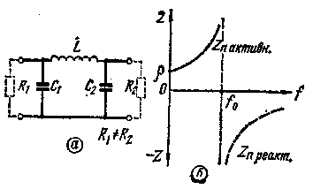
Fig.1
Another drawback of the P-loop is the dependence of its tuning frequency. As can be seen from Fig. 1,b, the characteristic impedance of the circuit is particularly strongly varies near its resonant frequency, which leads to the need of adjustment of the circuit even within the same range. When you transition to another range have to change the values of all items in connection with which such circuits are generally divided into three organ settings.
When using a modern, well-coordinated antenna-feeder devices, it becomes possible to perform the output circuits of the transmitter information.
If we consider the l-shaped, polozone bandpass filter type "K" (Fig. 2, a), we can see that the bandwidth limits the characteristic impedance of the filter actively and varies little depending on the frequency (Fig.2,b). However, this filter contains two inductors, and also requires that the load resistance were equal, which is impossible in the real world.
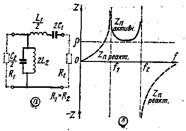
Fig.2
The elements of the bandpass filter are calculated as follows:
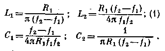
By successive transformations of the bandpass filter can be converted into a transformer filter (Fig. 3).
where L1, L2, C1 and C2 are calculated from equations (1).
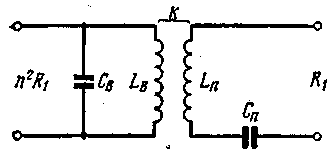
Fig.3
Converted the contour consists of two inductively coupled coils (located on the same frame) and two capacitors.
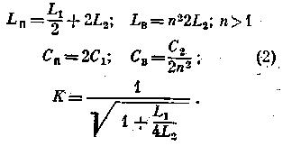
Calculations show that the value of the capacitance CB for all Amateur bands is approximately equal to the output capacity of the generator most of the lamps. Capacity of the JV turns out small, allowing you to replace it mindos capacity of the coils L and Lв. Practically, such a circuit may be designed as two inductors located on the same frame and connected inductive and capacitive connections (Fig. 4). The circuit can be switched as the output, and the input terminal of the cascade of the transmitter, if the final stage is made as a separate structure. In the latter case, the amplifier will have only one body configuration switch ranges. For a rational choice of frequencies of the local oscillator this circuit can be used in the mixing stages of the transmitter, thereby eliminating the necessity of adjustment and pairing intermediate stages.
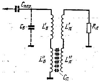
Fig.4
The calculation of the information of the contours produced in the following order
1. Choose the bandwidth of the circuit (frequency f1 and f2). To obtain a reasonably good values of the elements of the loop bandwidth should be at least 5% of the middle frequency range.
2. For the selected load resistance (wave impedance) is calculated according to the formulas (1) the values of the elements of the source filter.
3. Find the value of n2 for the selected load resistance and the required resistance of the anode circuit (obtained by calculating the output stage of the transmitter).
4. By the formulas (2) calculate the elements of the contour and the value of the coupling coefficient K.
5. Choose the frame and the wire diameter. For the windings L", L p and L"p when the transmitter power of 100 watts, you should Choose a wire not thinner than 1 mm. wire Diameter for winding L in can be taken smaller 1.5-2 times. It is best to use wire sew-2, having high dielectric strength.
6. Counting the number of turns of the bifilar winding L"and L"p to obtain the desired value of the joint Venture.
7. Counting the number of turns of the windings L and L in p (known by inductance).
8. The known coupling coefficient To place the windings on the armature.
Calculations for paragraphs 6, 7 and 8 are produced by well-known formulas available in radiotehniceskij directories.
The calculation is approximate, therefore, made on the calculation of the contours must be set in the real world. The setting is made by removing the variation curves of the anode current of the lamp when you change the frequency of the exciting voltage (Fig. 5).
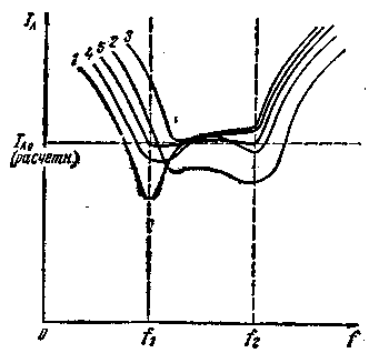
Fig.5
When removing curves, the circuit must be loaded on asyndetically resistor with a resistance equal to the characteristic impedance of the cable.
Suppose that the curve initially has the form 1. If you reduce the number of windings L p, the curve takes the form 2. If you move the coil L in (or part of it) up, the curve will take the form 3. Increasing the number of turns of the bifilar winding curve gives 4. Curve 5 corresponds to an appropriately configured circuit.
The table shows the number of turns of the coils, designed for the resistance of the anode load 3900 Ohm wave resistance of 50 Ohm feeder and frame with a diameter of 25 mm.
The rangeMHz
The number of coils, wire, mm
The distance between L and L in", mm
Note L"and L"p bifilar
L in
L p
3,5
14 sew-2 1,6
12 SEW-2 1,6 +56 SEW-2 0,5
24 sew-2 1,6
Close
L p on top of the bifilar winding
7
7 sew-2 1,6
4 SEW-2 1,6 +35 SEW-2 0.5
10 sew-2 1,6
5
The same
14
5 sew-2 1,8
21 sew-2 0.5
7+3 sew-2 1,6
10
3 coils L p
on top of the bifilar winding
21
3 sew-2 1.6
17 sew-2 0.5
7 sew-2 1,6
16
-
28
2 sew-2 1,6
12 sew-2 0.5
6 sew-2 1,6
25
-
Author: V. Kustov (UA3FN); Publication: N. Bolshakov, rf.atnn.ru