


")

Switching power supplies is not yet widespread in Amateur radio practice. This can be explained by their high complexity and accordingly the cost. However, in some cases, the benefits of these devices in compared to traditional transformer units - high efficiency, small dimensions and weight - can be crucial. The article described multiple pulse sources for various loads.
The dispute when choosing a power source (IE) for the particular instrument more often ends in favor of the traditional transformer blocks with continuous a method for stabilizing the output voltage as the simplest in the development and the manufacture. And the fact that they increased the size and weight, small efficiency, significant heating, almost into account are usually not accepted. The most an important argument is cost. In addition, there is a perception that pulse SP, especially the network, unreliable, create high frequency noise, more complex in the manufacture and adjustment, and roads.
These arguments are often traditional in those cases, when first designing the device, and then choose his SP from among commercially available. Thus often it turns out that the selected individual has not really suitable for the device: it heavy, very hot, and the equipment has become unstable.
Nothing like this happens, if the SP design for a specific device class equipment with consideration of the peculiarities of the input voltage and load. In this case some complications of IE, for example, the transition to the pulse method for stabilizing the output voltage, attach the device to a whole new level significantly improve its performance, which increases the consumer price of the whole device and pays for the cost of a complication of IE.
Below are some options network pulse SP, designed for specific devices taking into account peculiarities of the domestic single-phase network voltage of 220 V and frequency of 50 Hz. Results of operation for 5 to 7 years… they can be recommended to repeat the hams who are familiar with basic concepts of power electronics, principles and pulse control characteristics of the element base.
The principles of operation, manufacturing technology and electronic components PI specially selected loved ones, so most will be explained in detail basic PI, and the rest includes distinctive features.
In Fig. 1 shows a diagram of a single-channel pulse SP, designed for telephone sets with automatic opredelyaemaya (caller ID). It can be also suitable for other digital and analog devices permanent voltage 5…24 V and a capacity of 3…5 volts respectively, the current consumption which in the process varies slightly. IE protected from fault the output with automatic return to operation mode after the overload is removed. The instability of the output voltage when the input is from 150 to 240 V, the load current is in the range 20…100% of nominal and the temperature of the environment 5 to 40°C does not exceed 5 % of the nominal value.
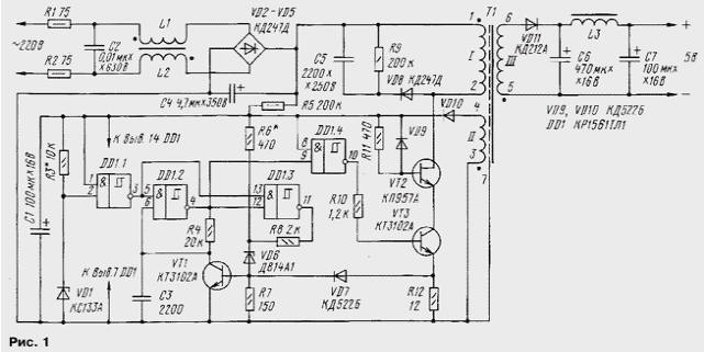
The input voltage supplied to rectifier VD2-VD5 through noise the filter L1L2C2 and resistors R1, R2, limiting the inrush currents when switching on IE. Actually high-frequency Converter is fed with DC voltage 200 340…In generated at the capacitor C4.
The basis of the inverter - driven pulse generator on the elements DD1.2-DD1.4, VT1 transistor and the Zener diode VD6. Source repetition rate pulses at the output of the element DD1.4 - 25…30 kHz, and pulse duration and pause (high and low) are approximately equal. If you increase the voltage on the capacitor C1 in excess of the value UC1 = UБЭVT1 + UVD6 Zener diode VD6 open, transistor VT1 during the pulse opens and drains rapidly the capacitor C3, reducing the pulse duration. This allows you to stabilize the output voltage of the PI.
The output of the generator controls the high-voltage switch on the diode and VD9 transistors VT2, VT3. Unlike traditional switches on one the bipolar transistor in which a control signal is supplied to its base, here applied chastnoe the connection of the two transistors high voltage VT2 and low-voltage VТ3. Typically, high voltage bipolar transistors - low-frequency, low-current transfer ratio base h21e and, therefore require high current administration. Here, the control signal served on a base of low-voltage transistors, high frequency with great h21e. When you open the transistor VТ3 in the base of the transistor through resistor VТ2 R11, a current flows, the opening and saturating it. When the transistor VT3 is closed, the emitter of the transistor VТ2 is "broken" and all his collector current flows through the base, the diode VD9 in the capacitor C1. Thus rapid resorption of excess charge in the base region of the transistor VТ2 and it force closes. In addition to performance reasons, this method the transistor control VТ2 (so-called emitter switching) extends the scope of its safe operation.
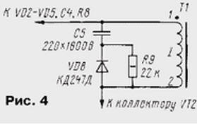
Elements C5, R9, VD8 limit the surge voltage at the collector of transistor VТ2.
The transformer T1 performs the functions of energy storage in pulse time and item galvanic isolation between input and output voltage. During of the transistor VТ2 winding I is connected to the energy source - the capacitor C4, and the current in it linearly increases. The polarity of the voltage on the windings II and III in this case is such that the diodes VD10 VD11 and closed. When transistor VТ2 is closed, the polarity of the voltage on all windings the transformer is reversed and the energy stored in it the magnetic field is transferred to the output smoothing filter С6L3С7 through the diode VD11 and in the capacitor C1 through the diode VD10. The transformer T1 should be made so that to magnetic connection between the windings II and III was the maximum possible. In this case, the voltage on all the windings have the same form and instant the values are proportional to the number of turns of the respective windings. If any reason the output voltage of the FE is reduced, it is reduced by the capacitor C1, which leads to an increase in the duration of the open state transistor VТ2 and, consequently, to increase the portion of energy transferred each period in the load - output voltage returns to its the original value. When increasing the output voltage of FE happens the reverse process. Thus the voltage on output.
The element DD1.1 is a control unit turning on the transmitter. When the input voltage of the capacitor C1 is charged through the resistor R5. The Zener diode VD1 is first closed, and the bottom (the scheme) input (pin 2) item DD1.1 voltage above the threshold switch, and the output DD1.1 - low level. This signal inhibits the operation of all units Converter; transistor VT3 closed. At a certain value of the voltage UC1 Zener diode VD1 is opened and the voltage at pin 2 is stabilized. The supply voltage of the chip continues to increase, and when UC1 = Uвкл the voltage at pin 2 of the Schmitt trigger falls below the switching threshold. The output element DD1.1 abruptly sets the high voltage level, which allows all nodes the Converter. Off same IP occurs when UC1 = Uвыкл < Uвкл because the Schmitt trigger has a hysteresis input. This feature is used to build host protection against short circuits on the output of a PI. When excessive increase the load current increases, the pulse duration, which causes the increase the voltage drop across the resistor R12. When it reaches the value UR12 = UVD7 + The UБЭ VT1 C 1.2 V, the transistor VT1 is opened and the transistor VТ3 closes. The pulse duration is reduced and, consequently, reduce the energy transmitted to the output. This happens every period. The output voltage decreases, which leads to a decrease in the voltage on the capacitor C1. Priznanie UC1 = Uвыкл element DD1.1 is switched on and off SP. Consumption the energy from the capacitor C1 controls almost Converter stops and starts charging through resistor R5, resulting in UC1 = Uвкл automatically PIS. Further, these processes are repeated with a period 2 4C…as long as the circuit is not resolved. Since the time Converter overload about 30…50 MS, this mode of operation is not dangerous and may continue indefinitely.
Types and component values shown in the scheme. The Capacitor C2 Is K73-17, C5 - K10-b (former designation CD-2B). Inductors L1, L2 and L3 is wound on the annular magnetic cores K10(6(3 from the press permalloy MP. Winding of the inductor L1, L2 contain 20 turns of wire PETV with a diameter of 0.35 mm and are located on each their half of the ring with a gap between the windings of at least 1 mm. Choke L3 wound wire PETV diameter of 0.63 mm round in a single layer (for the inner perimeter of the ring). The transformer T1 are the most important part of FE. The quality of the winding depends "surge" voltage at the collector of transistor VТ2, stability of the output voltage, the efficiency of the SP and the level of interference, so stay on the manufacturing technology. He performed on the yoke B ferrite MNM. All windings are wound on standard or homemade collapsible frame round wire and impregnated petv the BF-2. The winding I, containing 260 turns, wound around the first wire with a diameter of 0.12 mm in several layers. Its conclusions must be isolated from each other and the rest of the windings varnished cloth thickness of 0.05…0.08 mm to avoid breakouts. On the top layer of the winding is applied with glue BF-2 and isolate one layer varnished fabrics of a width that is slightly greater than the width of the winding to the turns of the upper the windings are not in contact with bottom coils. Next, the same wire is wound the shielding winding with one pin 7, put glue BF-2 and wrapped one by the same layer of varnished cloth.
The winding III of the wound wire with a diameter of 0.56 mm For output voltage 5 V it contains 13 turns. The turns of this winding is placed tight, with a slight interference fit, if possible in a single layer, coat with glue and isolate one layer of varnished cloth. The last wound coil II. It contains 22 of a coil wire diameter of 0.15 to 0.18 mm…laid evenly across the surface coil can be closer to the winding III. - Wound coil coat the top with BF-2, wrapped with two layers of varnished cloth and dried 6 hours at a temperature of 60°C. the Dried coil is inserted into the Cup, the ends of which also coat with glue, and connect them through a paper gasket ring mould thickness of 0.05 mm. Cups compress, for example, wooden clothespins from two sides the edge and again dried in the same mode. Thus, between the cups is formed non-magnetic gap. The coil leads are carefully isolated from the magnetic core.
During installation it must be remembered that the circuit involving pulsed currents needs to be shorter. Install the transistor VТ2 on the heat sink not required if heating it in real conditions of operation in the device is less than 60°C. otherwise specified, the transistor will be better to install on the heat sink area of 5…10 cm 2 .
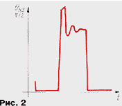
If all items are serviceable, adjustable SP is not difficult. To the exit connect the resistor 8…10 Ohm 5-watt, short the resistor R5, is connected to the capacitor C1 in accordance with its polarity adjustable a voltage source, pre-installing it Uвых = 0. Connected to the collector of transistor VТ2 oscilloscope with 1:10 divider at the input. Include source and increasing its voltage, fix the value at which occurred the inclusion of IE. On the oscilloscope screen should appear the signal frequency 30 25… kHz, the form of which is shown in Fig. 2. The selection of the Zener diode VD1 and resistor R3 sets the voltage on the device management IP within 7,3 7,7…V. the load should be constant voltage of 0.4…0.6 V. Disconnect the adjustable voltage source, remove the jumper from the resistor R5 and fed to the input of a PI network voltage. After a delay of 2…5 with IE is included, then measure the output voltage and the selection of the resistor R6 is set its value is 5 V. Next SP include rated load and make sure that in real operation conditions the transistor VТ2 and diode VD11 not heated more 60°C. this adjustment can be considered finished.
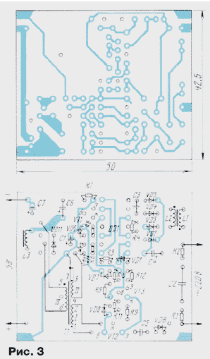
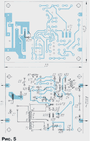
Design of IE can be different depending on the requirements the powered device. The author developed the design of minimum size and weight specifically for use in a telephone handset with caller ID. In the power supply used oxide capacitors "Weston" and "Rubicon" . All items except capacitor C4, is mounted perpendicular to the Board. The sizes of FE (50(42,5(15 mm) such that it can be inserted into the battery compartment phone "Technology" after some adjustments of the latter. Drawing of the PCB PI shown in Fig. 3.
IP was made by the author specifically to replace the traditional PSU B3-38, which were constantly observed failures. After replacement they stopped, and the phone works without shutting down almost six years.
Tests have shown that the output voltage SP begins to decrease when the input about 100 V. in addition, noise choke L1, L2 in the embodiment, the application with caller ID was not needed.
If the value of the output voltage of power supply source should be, for example, (assuming save output power), the number of turns of the winding III is necessary a proportionally increased, and the cross section of wire and the capacitance of the capacitors C6, C7 be reduced. The nominal voltage of these capacitors must be 30…50 % more output.
Heat sink transistor VT2 (if desired) in the case of installation on a specified IP the circuit Board is a metal plate size 48(10(Its 0.5 mm. set along a long side of the PCB close to the transistor VT2 through the mica strip and soldered to the specially provided for this the pads so that it was with good thermal transistor a contact. One can also use a heat-conducting paste KPT-8. It should be remembered that the heat sink is under high voltage.
In Fig. 4 shows part of the circuit SP power 10…15 watts output voltage 5…24 V Operation and settings of IE are not much different from discussed earlier. The adjustment and the method of changing the output voltage also similar. Of the differences we note the following. In this embodiment, the device is applied transistors VT2 - CTA, VT3 - CTA; diode VD11 - KDA, capacitors C2 - 0,015 µf ( 630 B, C4 - 10 µf ( ( 350, C5 - K15-5 and C6 set two capacitor 1000 µf ( 16 V; resistors R1, R2 - 33 Ohm 1 W, R6 - 200 Ohms, R10 1K R11 - 200 Ohm 0.25 W, R12 - 3.9 Ohm 0.25 W. All other elements the same as in Fig. 1. The inductor L3, containing 20 turns, is wound wire PETV diameter of 0.63 mm. Transformer T1 assembled on the yoke SW-8 ferrite MNS. Frame for winding - standard. After drying the coil set in the magnetic circuit, which is the same as in the previous case, stick together through the cardboard strip with a thickness of 0.2 mm. carefully Winding is wound in the same sequence. For option 12 In 1 And winding I contains 240 turns of wire of diameter 0.2 mm, winding II - 22 of the coil wire diameter 0.15 mm, winding III - 28 turns of wire with a diameter of 0.56 mm, the Shielding winding with one pin 7 is wound round in a single layer with a wire diameter of 0.15 mm For option 5 In 2 And diode VD11 should be CDS or 6ТQ045 (International Rectifier), and winding III - 13 of turns in the two wires with a diameter of 0.56 mm.
When mounting the transistor VT2 and diode VD11 must be mounted on heat sinks a minimum area of 50 cm 2 each, and the transistor VT1 and diode VD6 should be positioned at least 20 mm from the heating during operation the transformer T1. Other requirements are as for the previous IP. The author developed design SP minimum size to be set in the case of "block-fork". Drawing of the PCB of this option is shown in Fig. 5. Elements as in the previous case, is mounted perpendicular to the PCB and the the transistor VT2 and diode VD11 are on Board with the printed conductors flanges outward.
After Assembly and adjustment of the power source is set through the insulating mica strip on the heat sink, U-shaped aluminum 2 mm thick. Between your Board and the heat sink screws cylindrical wear sleeve with a height of 5 mm. Oxide capacitors selected "Weston" and "Rubicon", which reduced the dimensions.
During operation it is useful to connect the heat sink transistor VT2 (or a common the heat sink) through capacitors K15-5 3300 pF ( 1600 In each of the input conclusions. This measure helps to reduce radiated SP interference. Note, however, that heatsink is under high voltage.
Adjust SP is the same as in the previous case, but with nominal load SP cannot be enabled for a long time. The fact that the transistor VТ2 and diode VD11 heat up quickly, if you are without heat sink. SP with output voltage 12 In was used to power electronic clocks, and the output voltage 5 In - to power household computer "Sinclair". Malfunctions devices with the input voltage in the range of 120…240 V was observed. However, impressed by the size and weight of FE compared to their traditional counterparts execution.
In the PI stable amplitude of the pulse voltage on the secondary winding II of the transformer in the interval pause, so when the change of the load current and the significant influence of destabilizing factors the stability of the output voltage is relatively low. In cases where it unacceptable, you must use IE directly with stabilization of the output voltage.
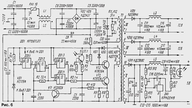
In Fig. 6 shows a diagram of a three-channel IC, the output voltage of the main channel which is stabilized due to the formation of a control signal on the deflection voltage of the channel of the nominal value, and the other two, additional, - like in the above sources.
PI is designed to power digital and analog electronic devices as from single-phase AC 220 V 50 Hz and DC voltage of 300 V. It is protected against short circuits in each of the outputs with automatic the return to operation mode when the overload. The temperature interval the environment in which IP works with natural cooling, - 0…50 °C.
The main parameters PI: input voltage - 150…240 V; output voltage - 5 In at load current 0…3 a, the instability of the output voltage when the maximum change in input, load current and ambient temperature 1 % of nominal value; 12 (0.02 To 0.2 A, 5 %); 12 V (0,1…1 A, 7 %).
IE is built from the same node as that of the previously described device. Output the voltage in the main channel (5 3 (A) stabilized with a managed source reference voltage on the chip DA1. Part of the output voltage with divider resistors R13-R15 serves on the control input (pin 17). When it the voltage will exceed the value of 2.5 V, through the anode (pin 2) current begins to flow, the led of the optocoupler U1 illuminates the phototransistor, the collector current of its flowing through resistors R5, R7, R9, R10, increases.
The voltage at the base of the transistor VT1 consists of two components: the fall the voltage across the resistor R9, R10 from the current flowing through the winding I transformer T1 and transistors VТ2, VТ3, and the voltage drop across the resistor R7 on the current of the phototransistor of the optocoupler U1. When the sum of these voltages reaches a value of about 0.7 V, the transistor VT1 is opened and the transistors VТ2, VТ3 closed, the pulse ends.
If the output voltage of the channel for any reason, exceed the value of 5 V, the phototransistor of the optocoupler is opened and the voltage across the resistor R7 increases. Since the voltage at the open of the transistor VT1 constantly, it drop on the resistors R9, R10, and hence the pulse duration reduced. As a result, the output voltage returns to its the original value. During the pause, when the energy of all secondary windings is transferred to the appropriate load, the voltage across winding V almost changed slightly (due to the change in the voltage drop across the diode VD11 and the coil wire when the current flowing through them). Therefore, the voltage on the windings III and IV in this time interval is changed slightly more than in the main channel. Thus, using only one feedback to stabilize the output voltage in several the channels. If the current of the main channel is changed is not more than twice a relatively the maximum value of the output voltage of the additional channels when constant load usually does not vary by more than 5 %, which is quite often valid. No other differences from the previously reviewed SP no.
Structurally, PI is the PCB size 110x60 mm double sided foil fiberglass with a thickness of 1.5…2 mm. Drawing the PCB is presented in Fig. 7. Transistor VТ3 and diodes VD9-VD11 mounted on Board with the printed conductors flanges outward. Ibid. is the jumper that connects the common point of the capacitors C1, C2 and the output minus the main channel. During final Assembly of FE this point it is useful to connect with heat sink, which is mounted on a mounted charge. The heat sink is a U-shaped aluminum bracket to which a plastic a cylindrical sleeve with a height of 5 mm is attached charge IE. Metal flanges the above-mentioned transistor and diodes are isolated from heat sink mica gaskets lubricated paste KPT-8.
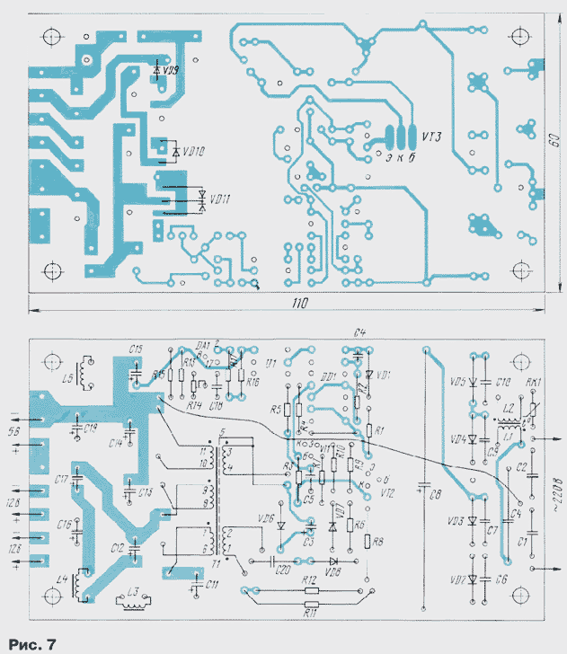
The thermistor RК1 - TR-10 for a current of less than 2 A. the Trimmer R14 - CP3-38A. Capacitors C1, C2 - K15-5, C4, C20 - K73-17; C6, C7, C9, C10 - K10-b (former designation CD-2B); C8 - C50-29.
Inductors L1-L5 is wound on the annular magnetic cores CHH,5 of permalloy MP. Choke L1, L2 are the same as in the previously considered PIS. Each of chokes L2-L5 contains 18…20 turns of wire PETV with a diameter of 1 mm. The transformer T1 is made on the yoke SW-10 ferrite MNS. All its made by winding wire PETV. Winding I contains 140 turns (4 layers) wire diameter of 0.28 mm, winding II - 12 turns of wire with a diameter of 0.15 mm, shielding - a single layer coil to a coil of the same wire. Winding III and IV contain 13 turns of wire with a diameter of 0.63 mm, and the winding V - 6 turns two wire of the same diameter.
First coil winding I, then shielding. Further winding of V, then winding III and IV at the same time (two wires). The last wound coil II. Each winding (or layer) isolate one layer of varnished cloth and impregnated with glue BF-2. After drying, the coil inserted into the magnetic core halves which stick together through the cardboard sheets with a thickness of 0.3 mm is also the BF-2 or fasten with special clips that are part of the magnetic circuit.
Regulate PI as follows. First resistor R1 sets the voltage the inclusion of the control device 10 10,5…V. After that, the outputs SP connect the nominal load, the fuse on the W And a current supply inlet a voltage of 220 V and resistor R14 set the voltage of the main channel 5 V. The output voltage of the additional channels is automatically installed.
PI can be used in single-channel version. Then he should be the main, involved in feedback.
The design considered PI such that during operation they should be installed in the enclosure, for example, inside the case of powered device. The last of the PI to be connected to the network via fuse IT on the current 3…4 A.
It should also be noted that the inclusion of all described IE no load the output voltage of the channels with parametric stabilization can significantly exceed the rated value, so if the operation is perhaps to the outputs you need to connect the Zener voltage stabilization 0.7…1 V greater than the nominal output or resistor resistance at 25…50 times the nominal load resistance.
Since IE all channels galvanically isolated, can be shared any of the output pins.
Described SP for a long time operated in two versions: a three-channel for computer power "Sinclair" with output parameters +5 In W A; +12 V 1 A; -12 V 0.2 A and a single channel for laptop power voltage of 18 V at a current of 2 A in the mode of operation, and in the mode of charging the internal battery. Failures, interference on screen monitors, any other differences in the operation of computers compared to their work from the "brand" of FE was observed.
Author: A. Mironov, Lyubertsy, Moscow region.