


")

The main purpose of the device described here - the power of personal computer. But not only. It is suitable for powering many other Amateur radio development of increased capacity, for example, USC.
The principle of operation of the proposed power supply (Fig. 1) is the same as that of the blocks power color TV third generation. It also works in mode, close to the intermittent mode currents and, hence, is self-oscillating device. But there is a fundamental difference: it applied "emitter switching" powerful switching transistor that allows you to use them in a wider frequency range and, in addition, reduces the likelihood of failure of the high-voltage transistor.
Experiments confirmed that transistor CTA a switch transistor KTA its emitter circuit works well even at a frequency of 120 kHz. Another advantage of the PSU - the possibility of using it in a wide range of output current.
The device is a single-ended voltage Converter with reverse the inclusion of a rectifier diode. The output voltage of the channels of the block is stabilized by changing the duration of the open state of electronic transistors switch.
Key components of the source unit: rectifier network the voltage filter, single-ended Converter with output filters, a pulse-width controller, the error amplifier and auxiliary switching regulator.
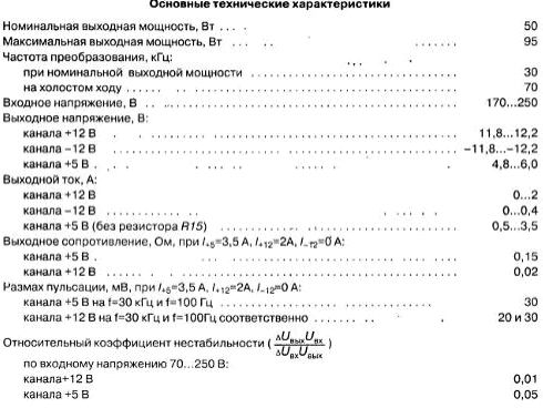
Mains voltage passes through a noise filter formed by inductors L1, L2 and capacitors C1, C2, rectified by a diode bridge VD1 VD4 and… through the resistor R1 rectified voltage is supplied to a smoothing capacitor C7. The Capacitors C3 C6… weaken the penetration of interference in the network, and the resistor R1 limits the throw of the input current at the moment of switching power supply. Converter starts after about 0.1 s after connecting the unit to the network that a few facilitates the work of the rectifier.
The main components Converter - pulse transformer T1, a powerful high-voltage switch transistors CTA (VT1) and CTA (VT2), rectifiers and output the filters. Transistor CTA (with a large maximum allowable voltage collector-emitter) opens and closes the circuit and opening its emitter circuit high-speed transistor CTA that prevent the occurrence of secondary breakdown and reduces the duration switch emitter of the transistor. This allows you to adjust the output the voltage in a wide range without alteration of the pulse transformer.
Resistors R11 and R12, total which resistance is 0.5 Ohms, and serve as a current sensor Converter. When VT1 transistor closes, the current of its collector through the diode VD6, the Zener diode VD5 and the capacitor C8 is shorted to the negative output of the rectifier bridge VD1 - VD4.
Diodes VD13-VD15 - rectifiers the pulse voltage of the secondary windings 3, 4 and 5 of the transformer T1 . Ripple the output voltages of the rectifiers smoothed by capacitors C13-C18, LC-filters L5C21, L6C22.
Resistor R15 connected the channel output +5 V, prevents excessive increase in the voltage across it when channel loading +12 V. with this resistor, the voltage at the channel output +5 In no load does not exceed 6 In, safe for computer chips, at a current load channel +12 V to 2.5 A. the Voltage channel-12V stabilized integrated stabilizer DA2.
Amplifier the error is connected to the output channel +12 V. Source model voltage is the output of the stabilizer DA2. The transistor amplifies the signal VT4 error. Load transistor serves as the led of the optocoupler U1, and the diode protects VD17 its emitter junction. When the voltage on the channel output +12 more than 12 In the led of the optocoupler is turned on and thereby increases the current through the phototransistor of the optocoupler.
Open state transistor VT1 switch is determined by the charging time of the capacitor C11 (approximately 4 to +1) the current of the phototransistor of the optocoupler. The larger the value of the current of the phototransistor option, the faster charging the capacitor. 11 and the less time the transistor VT1 is in the open state.
After connecting the unit power to the network begins to charge the capacitor C8 via the resistor R2 and diode VD6). When the voltage across it reaches 4.5 V, the current flowing through a resistor R6, a Zener diode VD12, the emitter junction транзистораVT2, resistors R11, R12, and through resistors R6, R5, emitter the transition of the transistor VT1, VT2 transistor and resistors R11, R12, translates switching transistors in active mode. The positive feedback signal communication between the windings I and II of the transformer T1 through the diode VD7, capacitor C10 and resistors R5, R7 quickly opens the switching transistors. Begins the accumulation of magnetic energy field in the magnetic core of the transformer T1. After a certain period of time the transistor VT3 opens and closes the transistor VT2, and hence the transistor VT1. When this transistor VT3 summarizes the voltage supplied to its base from the current sensor R11, R12 and capacitor C12.
At startup or in case of overload the inverter when the voltage drop across the resistor R11, R12 exceeds 1 V, the transistor VT3 is opened by the current flowing through the resistor R10 and diode VD11, so the device can withstand momentary overload. With the closure of any of its channels to the common conductor of the power supply automatically switches to limiting the power is not leaving the building. In normal Converter operation the time of closing switching transistors is determined by the duration of the charging of the capacitor C11.
After closing of powerful transistors, the polarity of the voltage on the windings pulse transformer is replaced by the opposite, and thus the diodes VD13…VD15 be included in the forward direction and the rectified current charge capacitors LC-filters. When the value of this current will be close to zero, in the resonant circuit, formed by the coil / transformer T1, its parasitic capacitance and capacitor C9, electrical oscillations occur. The first one opens power transistors switch - described process is repeated.
While the transistors VT1 and VT2 are closed, the voltage on the lower circuit on the output winding of the transformer II is relatively sub-zero of the output capacitor C7 and negatively through resistor R8 and diode VD8 securely holds the transistor VT2 is in the closed state. Minimum the voltage on the base of this transistor is determined by the voltage stabilization the Zener diode and voltage VD12 the diode VD10. Through the circuit is charged R8VD9 and the capacitor C11 And the cathodes диодовVD8 and VD9 United, then the voltage across the capacitor C12 may not be less than the base transistor VT2 (i.e. about -4 In).
The voltage at the channel output +12 V stabilized by the method of pulse-width regulation. It simultaneously stabilizes the voltage and channel +5 V.
However, as a pulse transformer, diodes and some other elements the device is perfect, the stability of the output voltage of the channel low. Therefore, the applied auxiliary switching regulator, which performs two functions: it provides a channel +5 In a portion of the load current for stability voltage and load the channel +12 V if it is not loaded.
The composition auxiliary stabilizer includes integrated stabilizer DA1, chokes L3, L4, capacitor C19, diode VD16, resistor R14 chip DA1 is electronic switch, a source of reference voltage and amplifier the error signal. The inductor L4 and the diode VD16 - required attributes switching regulator. The excitation circuits DA1 provide the inductor L3 and capacitor C19 and resistor R14, reducing the factor of the circuit L3C19, prevents the occurrence of high-frequency oscillations.
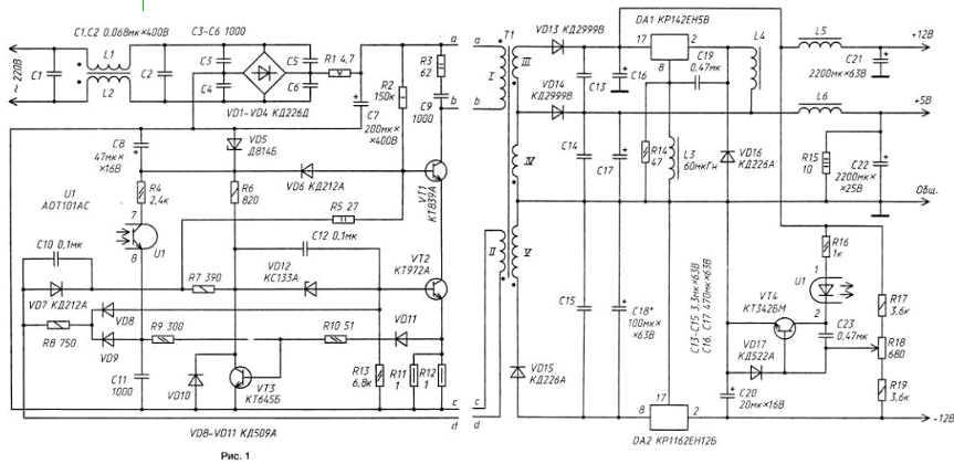
All elements of the unit power mounted on the PCB size mm 205x105 (Fig. 2) of one-sided foil fiberglass with a thickness of 1 mm.
The main parameters of the resistors and capacitors are marked on the schematic diagram in the device. Transistor CTA (VT1) replace KT838A, CTA, CTA, CT and CTA - CTB. Instead transistors CTB (VT3) and CTB (VT4) can work similar transistors with current transfer ratio base not less than 50. OPTRON AOTUS (U1) replace on AOTS, AOTA or AOTA.
Diodes KDA(U, VD7) replace CD or CD with any letter index, and CDV (VD13, VD14) others, with similar characteristics, for example, series CD, CD, CD, CD. Instead of the diodes VD1-VD4 rectifier the bridge will fit CDG or in an extreme case - series CD reverse voltage at least 400 V.
Through the Zener diode DB (VD5) significant current flows that should be considered when his replacement is valid for the current should be at least 40 mA. Large currents flowing through the capacitors C16-C18, so preferably they have a series C50-29, K50-24. Rated the voltage of the capacitors C1-C6 (CD-2, C-2, K73-16, etc.) shall not be less than 400, they should avoid working with the variable component of at least 350 In at the frequency of 50 Hz. Capacitor C9 is C-2 nominal voltage of 1600 V. the Rest of the details are not critical to the replacement.
Transistor VT1 set on a heat sink with a surface area of about 200 cm2, diodes and VD13 VD14 - on the sinks area of 45 and 35 cm, respectively, and the stabilizer DA2 - the heat sink area of 70 cm2.
The Transformer T1 formed on the yoke. Ø 12x15 ferrite 2000NM, with non-magnetic gap of 0.5 mm Winding I contains 160 turns the PEV-2 0,47, folded double. Winding II - 4 turns of the same wire, but folded into three sections. To improve the magnetic coupling of the windings III and IV made copper tape with a thickness of 0.2, a width of 27 mm and contain 3 turns. Copper tape you can replace the wire sew-1 0,8, folded in three. Winding V contains 8 turns of PEV-1 0,4, folded four times.
Inductors L1 and L2 are wound on a common magnetic core size of CHH ferrite 2000NM and contain 35 turns of PEV-1 to 0.4 each. The magnetic cores of the inductors L5 and L6 are the segments of the rod of ferrite MN with diameter of 8 mm and a length of 20 mm; each of them contains 15 turns. The inductor L4, made in armored cores. <url> ferrite 2000NM (with non-magnetic gap of 0.5 mm), contains 35 turns of PEV-1 to 0.8.
Accurately mounted power supply, usually starts to work without pre-build. But, in order of insurance, the first connection to the network, it is desirable be made through the incandescent lamp capacity 15…25 W, calculated on a voltage of 220 V. once the Converter starts, variable resistor R18 is necessary to set the channel output +12 In the corresponding voltage.
If the requirements for the supply voltage of +5 V tougher (or more output current), the error amplifier must be connected to the channel output +5 V this upper circuit the terminal of the resistor R16 and R17 have connect to the output conductor channel, +5 V, for example, to the positive conclusion capacitor C17, and also to reduce the resistance of resistor R16 to 300 Ohms, and resistor R17 - up to 1.5 ohms. Stabilizer DA1, inductors L3 and L4, a resistor R14, capacitor C19 and diode VD16 thus excluded. However, after such modifications, the voltage at the channel output +12V with the increase in the current channel +5 V will also increase, so the voltage this channel will be stabilized (for example, using chip CREB).
The undesirable increase in voltage channel output +5V can be prevented by connecting in parallel the capacitor C17 the second led of the optocoupler U1 through Zener XA and resistor 180…200 Ohm. With the pins 6 and 7, and conclusions 5 and 8 of the optocoupler should be merged. This will not only protect unit power from exceeding the output voltage, but also improve the reliability of its operation as in this case, the feedback circuit will be duplicated.
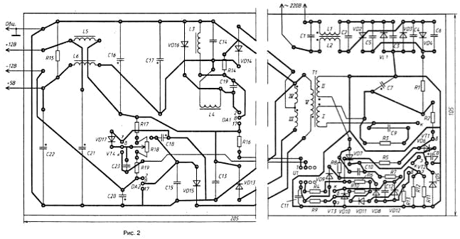
The described device is applicable to power many other Amateur radio structures, such as power amplifiers CC. It is only necessary, given the characteristics of specific electronic device to rebuild the secondary side of the unit power, and the change of 1.5 times the output voltage regulation is achieved the signal level of the feedback winding of the transformer T1. A concrete example. To power the power amplifier based on the chip CAN the correct source of the bipolar voltage ±15 V. In this case the secondary of the power supply can be collected by the circuit shown in Fig. 3.
Winding III and IV of the transformer T1 contain 7 turns of copper tape with a thickness of 0.1 and a width of 27 mm or wire Sew-1 0,8, folded into three sections. The winding, both windings carry out simultaneously. Conclusions 6 and 7, and 5 and 8 optocoupler U1 needs to be combined.
Literature
Author: D. Bezique