


")

In we offer our readers the article description and principle of operation practical scheme SMPS based cascaded flyback voltage Converter. No discharge voltage at the drain of the field the switching transistor makes it possible to reduce the requirements for its the maximum allowable voltage.
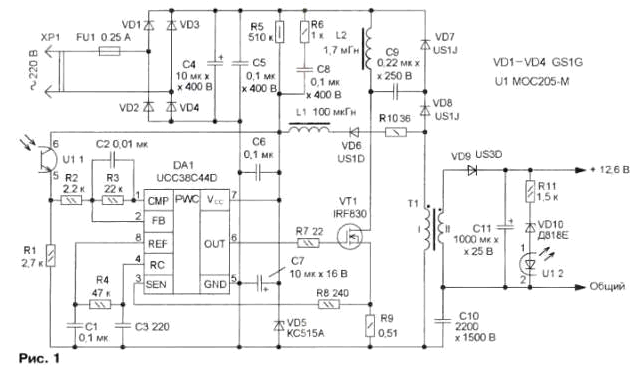
Network switching power supply, the circuit of which is shown in Fig. 1, refers to the so-called flyback converters, but his scheme the output stage is substantially different from the "classic" flyback. You will notice that the chain in stock transistor VT1 no the damping diode-resistor-capacitor circuit to power the controller does not requires a separate winding of the pulse transformer, and in return he applied two separate energy storage element, an inductor L2, and the isolation transformer T1.
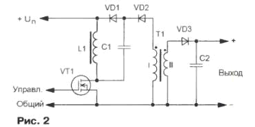
In the output stage, a simplified diagram of which is shown in Fig. 2, the process of energy transfer can be divided into two stage. The first is the energy is accumulated in the magnetic field of the inductor L1 in the time of forward stroke and passed through an open diode VD1 on the capacitor C1 during the return stroke. By the end of the flyback capacitor C1 will be charged. his upper circuit plate will become negative relatively lower potential. At the second stage during the next forward stroke the charged capacitor C1 through the open transistor VT1 and diode VD2 is connected to the primary winding of the transformer T1 and will be discharged. At this time there is the accumulation of energy in the magnetic field of the transformer T1 and, finally, during next flyback energy is transferred to the output through a rectifier diode VD3 and smoothing c the capacitor C2.
We now analyze the the operation of the SMPS (see Fig. 1) in more detail. The diodes VD1-VD4 assembled bridge rectifier, capacitors C4, C5 smooth out the ripple of the rectified voltage. Since the processes of accumulation of energy, combined, through the open transistor VT1 proceeds total current of the inductor L2 and the primary winding transformer T1. The current in L2 increases linearly under the action of the rectified voltage, and its rate of increase is determined by this voltage and the inductance of the inductor. Linearly increasing the current in the primary winding T1, and the capacitance of the capacitor C9 is selected such that during the forward stroke, the voltage at it varies slightly. This component of the current of the transistor has the same direction as the current of the inductor, as to the upper circuit the output winding of the primary winding of the transformer T1 applied voltage negative polarity.
When the current through the transistor VT1 reaches a certain value, the voltage at the resistor R9, which functions as a current sensor, will cause the switch the master controller DA1 and field-effect transistor is closed. Note how the disadvantage is the fact that at the same power level with a "classic" flyback Converter current of the transistor. The advantages of the device are shown on the reverse phase progress - as of the closing field-effect transistor VT1 current the inductor L2 through EMF charges the capacitor C9. Since the voltage on this the capacitor cannot change instantaneously, the transition process at the drain transistor flows smoothly, the release voltage is missing, so there is no need to use damping the diode-resistor-capacitor circuit, substantially reduce efficiency power source for small values of output power.
With the beginning of the return stroke stops the process of storing energy in the transformer T1, and the voltage at its primary winding, which during the forward stroke was negative, due to the self-induction will be a plus - opens diode VD6, providing the supply voltage to the controller DA1. and diode VD9. nourishing load. When connected to the mains power supply controller original flows through the circuit and R6C8 limited by the Zener diode VD5 on 15 V. the Resistor R10 limits the current of the Zener diode in the steady state, and the inductor L1 additionally protects the power circuit of the controller from power surges. Frequency conversion set elements R4, C3 and is about 62 kHz. The output voltage is controlled by the opto-coupler U1 and regulated by changing the duty cycle of the control pulses arriving at the gate of the transistor VT1.
The SMPS provides the output voltage of 12.6 V at a current of 0.5 A.
The instability of the output voltage does not exceed ± 2,5% and its ripple on the conversion frequency does not exceed 100 mV efficiency when the output power of 6 watts is not less than 0,72. If the load of the SMPS operates in restart, the output voltage is not increased. Minimum load, in which it is included in the stabilization mode, can serve as the indication led. Consumed by the network the current in this mode is reduced to a few milliamps.
The device was assembled on two prototype printed circuit boards. One of them - controller with DA1 related elements on the second - the rest.
The boards are interconnected by wires short as possible. On the controller Board used resistors and capacitors SMD size 1206.
Capacitors C5, C9 - K73-17, C4, C11 - suitable for the size and working voltage oxide capacitors. Choke L1 - ES, resistor R9 is composed of two connected in parallel, and R5 or two connected in series. MOSFET IRF830 replace on another field switch to the allowable voltage for the source-drain 500, a current of 4.5 a and the resistance of the channel in the open state is not more than 1.5 Ohms. Heat sink for the transistor is not required. The device incorporates chip UCC38C44D by Texas Instruments. With small changes in the schema you can use similar controllers from other families, including and UC3844A. It is important to maximize the fill factor of the output pulses was equal to 50%.
For the manufacture of the inductor L2 and transformer T1 used small W-shaped magnetic EFD15 data sheets, material No. 87, complete with standard frame. the inductance of a single turn is 100 NH. The inductor L2 contains 130 turns of wire sew-2 0,2, stacked in four layers and has an inductance of 1.7 inst. You can also use an inductor with a saturation current of 0.3…0.4 A, for example, SDR1006-152KL Bourns company. The transformer T1 includes two windings 36 turns of wire Sew-2 0,35 isolated from each other with two layers of polyester tape. the inductance of each winding - 0,12 mH. The use of these cores allows you to gain height the mounted device about 10 mm.
For transformer it is also possible to apply ring the magnetic core of material MP-140 with an outside diameter of 18 mm, the efficiency is reduced by 2…2,5%. In this case, the number of turns should be increased to 50, and winding easier be wound twice a folded wire with high quality insulation, for example, MS-14 or M-12.
Made this the transformer has a lower leakage inductance, and the device working with him more stable.
Since most elements of the device are energized network, for establishing and verifying it is desirable to apply a suitable power isolation transformer, connected to the output establish SMPS equivalent load. Preliminary it is necessary to verify proper operation of the controller and its circuits, which, without attaching device to the network, temporarily served between the power pins of the controller of the permanent voltage 13…14 V. the gate of the transistor VT1 needs to attend the pulse is a square wave with frequency conversion.
Selection of elements and establishing the device does not require. to change the output voltage in small the range is possible by selection of the resistor R11 (1.2 kω). Connecting to the output of the rated load, check the output voltage and turning off the SMPS, shorting it out. The average current consumed by the network, when this should decrease, indicating normal operation of the protection circuits.
Author: V. Sokol, chashnikovo Solnechnogorsk district, Moscow region.