


")

The article describes a switching power supply controlled by a specialized microchip. The device is equipped with a standard pulse transformer from TV blocks.
It would seem that the sources of supply (PS), which are integral elements absolutely all electronic devices must be least susceptible rapid changes - in fact they have existed for more than half a century. But the development of modern technical solutions and not shy away from this very large area electronics.
First, traditional SP battery was replaced tube network with LC-filters, and then transistor and integrated linear stabilizers regulation.
The struggle for efficiency and improvement of weight and dimensions contributed to the development and implementation of pulse SP (SMPS). Along with semi - and the full-bridge SMPS widespread flyback sources, because without special measures the risk of a through current in bridge SMPS (due to flow in one arm of opening voltage when because of its inertial properties of the other shoulder has not fully closed) always led to the work of the switching elements in the real circuit and failure of the expensive high-voltage transistors. These special measures greatly complicated bridge SMPS, and therefore in household appliances wider widespread flyback SMPS, in which the switching transistor in the first cycle provides accumulation of electromagnetic energy in the windings and the cumulative magnetic core of the transformer, and the second transmission load. To verify the relative complexity of such SMPS, enough look at the diagram of the power module MP-403 TVs ZUSTST, USCT or cassettes scan and power of the if-501 TVs USCT.
And only the latest development specialists from Siemens and domestic of the manufacturers that produced the chip to control a flyback SMPS ТDA4605 (domestic analogue CREW - the so-called PWM controller), significantly simplified hams with the task of developing a highly reliable and economical SMPS. Although reference [1], containing information on the PWM controllers, and not free from some of the errors, we should note its great value for constructordeclaration SMPS. In the manual [2] describes the SMPS in TVs the 6th generation using domestic chip CREW, but there is no background information (voltages, waveforms of signals), describing her work. Unfortunately, none of these sources are not given winding cumulative parameters of the transformer. However, using available data, in Amateur radio purposes always it is possible to adjust an existing pulse transformers to create the necessary modern SMPS. To solve this problem will help the materials published article, they can also be useful for radio Amateurs involved modernization and repair of domestic and import video.
Service functions performed by the chip is extensive:
- "soft" launch of the SMPS with a continuously increasing the duration of the starting pulses;
- stabilization of the output voltage in operating mode control duration the switching pulses;
- "snap" the beginning of a switching pulse to the time of completion of transmission the stored energy to the load;
- protection SMPS at idle and circuit in the load;
- disable SMPS when voltage variations in excess of the prescribed limits;
- suppression of spurious oscillatory processes initiated cumulative transformer;
- thermal protection (disable the chip when the case temperature above +125 °C).
Functional assignment of the pins are listed in table. 1.
Table 1
Pin number The functional purpose 1 The input of the control amplifier 2 The input signal simulating the change in the cumulative current in the winding transformer 3 The input divider network voltage to turn off the switching pulses dierent from the valid values 4 The General conclusion 5 The output of the switching pulses 6 The supply voltage of the chip 7 Input for connecting the integrating capacitor, Manager pulse width of the soft start SMPS 8 The input signal to determine the zero-crossing pulse in the secondary windingKey features
The voltage, V 7,5 13… The switching frequency of the switching pulses kHz, no more than 165 Power SMPS (determined by the type of magnetic circuit and parameters switching transistor), W, not more 250 Input voltage control amplifier, 0,37 0,43… Limits of change of commutating voltage to recharge capacity the gate-source of the switching MOS transistor, -0,3…+6 Limits of change of commutating current, And to 1.5…+1,5The control amplifier is the main element of the chip. Receiving a signal from the an additional winding of the transformer and comparing it with the internal model voltage, it generates the switching pulses of different duration, which is determined by the values in the load current and the rectified mains voltage. The pulse duration is changed in such a way as to maintain a constant the output voltage of the SMPS.
The main element SMPS - cumulative pulse transformer, which, in principle, can be any. Wide range of output voltage regulation, provide a microchip and a large set of output windings transformer facilitate the task of creating a SP with required parameters. It is advisable, for example, to consider the use of pulse transformer The TPI-8-1, previously described in the magazine "Radio" [3].
Diagram of SMPS, based on [1,2] and tailored to the application specified transformer depicted in Fig. 1 (unused winding transformer not shown, the terminals 4 and 10 were absent initially).
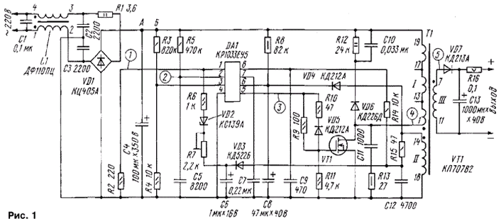
The apparatus comprises a noise filter, which prevents the penetration in the supply network of high frequency interference (L1, C1-C3); current limiting resistor, limiting the inrush current when you turn on the SMPS (R1); bridge rectifier network voltage (VD1); a voltage divider in the feedback circuit of the Manager amplifier circuits forming the stabilization level of the output voltage of the SMPS (R2, R6, R7, VD2); filter in the power supply circuit SMPS for low pulsation input voltage (C4); a voltage divider for monitoring changes in the network voltage and turning off the SMPS at an unacceptable vibrations (R3, R4); sawtooth generator to simulate the variation of the current in cumulative windings of pulse transformer (R5, C5); shaper pulses in the circuit of the feedback signal (VD3, C6); an integrating capacitor in the control circuit soft start SMPS (C7); filter capacitor circuit power chips (C8); current limiting resistor in startup mode the chip before its release to the operating mode (R8) rectifier voltage, supply the chip connection from winding (II) of the transformer in operation (VD4); chain feed pulses to control the switching transistor (R9-R11, VD5); chain to limit peak voltage spikes at the drain of the transistor (VD6, R12, C10); the damping circuit for eliminating spurious oscillations (C11, R13); noise filter in the chain determine the beginning of the measure of formation a switching pulse (transition of the output voltage pulse through zero) and feedback control amplifier (R14, C9, R15, C12); the rectifier and the filter output voltage (VD7, C13); current limiting resistor in the circuit output voltage (R16).
The test results of devices with different output windings and the values of used items, shown in the diagram, to obtain the output voltage 12 V at load current of 1.25 As shown in table. 2.
Table 2
Winding III Voltage, V 7-11 12,5 16-20 8 3-5 2,2 8-12 10 6-12 55For an output winding, one should use table. 3 containing parameters of the copper winding wires, which are most often used in pulse transformers. Winding III, designed for a voltage of 24 V At "regular" use, contains 16 turns of three parallel connected conductors PMTL-0,35. The total cross section is about 0.3 mi equivalent to the conductor diameter of 0.62 mm For the current density of 4.25 A/mm2, the corresponding temperature rise of the transformer at 30 °C, the allowable current in the winding is 1.28 And that satisfies the requirements (calculator, item conductors easily continue the direction of increasing and decreasing diameter). If you use the windings V and VI (findings 14, 18 and 16, 20 respectively [3]), connecting them in parallel, the output SMPS can get the current up to 3.5 A.
Table 2
The diameter of the insulated wire, mm Diameter of copper, mm The allowable current, And 0,41 0,35 0,41 0,44 0,38 0,48 0,47 0,41 0,56 0,5 0,44 0,65 0,53 0,47 0,74 0,55 0,49 0,8 0,58 0,51 0,87 0,6 0,53 0,94 0,62 0,55 1,01 0,64 0,57 1,08 0,66 0,59 1,16 0,69 0,62 1,28 0,72 0,64 1,37 0,75 0,67 1,5 0,77 0,69 1,59 0,8 0,72 1,73As in the power module MP-403, cumulative winding is a winding I (pins 1, 19). Special attention should be paid to the correct connection (phasing) conclusions (usually on the schemes start winding always denote a point). Rooms conclusions additional winding connection and power the chip shown in Fig 1.
It should be borne in mind that the operating current in the coil depends on context the total power of the load and not necessarily reaches the maximum value 1.5 A. When assessing the operating voltage windings to remember: proportional relationship between the number of turns and the voltage observed only the secondary windings and primary windings, as they working in different half-cycles (cycles) pulse voltage, and the ratio between their voltage will depend on the duty cycle of the switching the pulses.
The dummy load when establishing three parallel connected resistor, PMT-25 resistance 30 Ohms each. Before applying mains voltage to be included in the open circuit between points A and B (Fig.1) ammeter 0.5 A. It is used here not only as a measuring device, showing the reaction device for changing the values of elements (an increase in input current will be to indicate the increase of the load current or voltage in the secondary the windings), but also as a reliable indicator power-on silent working SMPS. This prevents accidental electric shock when establishing.
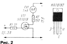
It is also useful to check the correctness of the switching transistor, gathering the simplest measurement circuit according to the scheme of Fig. 2 (ibid shows the Pinout of the field transistors KV, KB and their foreign counterparts IRFBC30, IRFBC40, BUZ90A, 2SK1221, etc.). Increasing increments of 0.1 V, the voltage at the gate of the transistor, make sure that starting from the threshold voltage (1…5 V depending on type and parameters of the transistor), the current in the circuit runoff gradually increases and reaches 500 MCA approximately 0.5 V after opening. Better to use a power supply with a protection current, pre-installed on the 1 mA level. This will eliminate damage to the transistors even when connection errors because of their unknown the Pinout.
After taking those preparatory activities trimpot resistor R7 should be set to the middle position and included in the network of SMPS. During establishing the device is better positioned on the desktop elements down: then the printed circuit Board will protect from injury during a possible explosion oxide capacitors as a result of excess voltage due to improper connection the windings.
When there is insufficient secondary windings of the output voltage for the SMPS to work the mode will hear clicks transformer with high tone ("cyganie"), due to the periodic inclusion of the start mode on increases to the threshold voltage on the capacitor C8. In the process establishing SMPS first need to check the influence of the position the movable contact of the trim resistor R7 on the parameters of the output pulses.
You should be very careful approach to the selection of the parameters of the circuit elements the sawtooth formation (R5, C5), which determines the maximum the duration of the open state of the switching transistor. The voltage at the capacitor C5 in the chip is compared with the voltage at the input of the Manager amplifier, and the switching pulse is terminated when they coincide. If these the elements chosen incorrectly, you disable SMPS from the network reduction the voltage at the output of the filter network power will be offset by an increase in the duration of the switching pulses and exceeding the allowed values stock current of the transistor, leading to permanent damage.
In the process of building to connect the SMPS to the network should use reliable switching elements (switches, switches and not the plug and socket), since emerging contact bounce may be the cause of failure of the switching transistor.
After establishing the device must surely go to work the mode will be indicated by the silent operation of the SMPS and indications control of the ammeter in the range of 100…350 mA depending on load. If this does not happen, then the device is defective items or admitted errors in the installation.
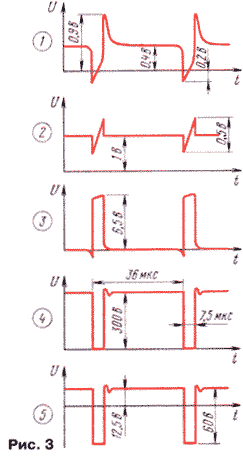
Through the first few tens of seconds of operation of the SMPS must be disconnected from the network and to control the thermal regime of the transistor, transformer, diodes, then repeat the same after a few tens of minutes of work. In the absence of overheating it is necessary to adjust the output voltage and to control the shape of the signals in accordance with Fig.3.
Analysis of the operation of the device showed that when using a ready pulse transformer cumulative winding are better left unchanged, and the winding connection to select a voltage of 8…9 when In "normal" use, i.e. for transformer TPI-8-1 required winding connection containing six turns (winding with the pin numbers 14 - 18).
It may be that the selected transformer does not provide the required the parameters of the SMPS, thereby requiring replacement of the secondary winding. Hard manufacturing technology of pulse transformers (distribution of the windings in strictly specified order, the clearances between the edge of the winding and the outer side of the frame, the diameter of the wires depending on the operating current, distribution of partial layer "vrazrjadku" across the entire width of the winding for the purpose of creating a uniform magnetic field within the working volume of the transformer) is required when the manufacture of special care and accuracy in the Assembly. But dismantling transformer, glued together with epoxy glue, is almost impossible without the use of milling equipment (after cutting cutter the transformer will need to restore the working gap at the Central core of his with the reduction of the thickness of the cut). So the only way to create situation - soldering electrostatic (noise) of copper screen foil, removing unnecessary windings and winding in their place "Shuttle" method the required winding, and instead of a wire of a large diameter is more preferably the use of multiple parallel conductors with smaller diameter equivalent to the total cross section.
The device is equipped with non-deficient parts. Capacitors C1 K73-17, C2, C3, C10, SP - K73-9, all at a nominal voltage of 630 V, C4 - C50-32. If the load is SMPS exceed 50 watts, in parallel with the capacitor C4 is necessary to connect another the same or use a C50-35B with a capacity of 220 µf (or 330 µf) voltage on 350 V. the Capacitor C6 - K53-30 or another. Oxide capacitors C8, C13 C50-35. Other - any ceramic rated voltage 63… 100 V. All fixed resistors - MLT, except R16 C5-MW. The trimmer R7 - SDR-386. The diode bridge will replace CCB, CCW or individual diodes with permissible reverse voltage of at least 400 V and an operating current of 1 A. the Diode VD6 and VD7 - pulse with a nominal frequency of not less than 35 kHz, and the first of them on the nominal voltage of at least 600 V and a current of 1 A, the second - 100V and 5 A (for low voltage SP). Instead of industrial choke mains filter L1 is applicable homemade: use a ferrite ring RM-2000NM an outer diameter of about 20 mm with a wound windings on it in a few tens of turns of the two conductors MGTF is 0.35.
All elements of the SMPS are mounted on the PCB of unilateral foiled fiberglass 1.5 mm thick (Fig. 4). Into the holes A and B Board solder the jumper after the establishing of the device. Capacitor C4 is fixed parallel to the Board with a wire clip that is installed on the recess in the end portion of the housing; the ends of the yoke sealed in appropriate the holes. Terminals of the capacitor to ensure the reliability electrical contact is connected to the Board through the washer with a petal and a nut on the threaded body portion. A capacitor C and a resistor R13 connected in hinged circuit, a second terminal of the capacitor with solder mounting petal connected directly to the metal plate of the casing of the transistor, mounted on the heat sink. This will significantly reduce the level radiated interference. With the same purpose SMPS placed in a metal housing with ventilation holes for cooling.
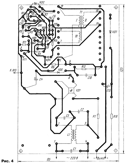
To the network device connected flexible circuit wire in the gap of one conductor being served to the switch and fuse trip current, in two times the work, measured by the ammeter during the build (as noted earlier, it will depend on load). The secondary winding is connected flexible insulated conductors depending on the desired value output voltage of the SMPS. Transistor VT1 is shifted to the boundary of the fees that it it was possible through the mica plate is fastened directly on the metal the body of the device or to the heat sink with the effective cooling area 100…200 cm2.
It should be remembered that the SMPS is galvanically coupled to the network, by careless handling this can be a cause of electric shock. According to the rules equipment electrical safety at the time of establishing the SMPS must be connected to network via an isolation transformer with a capacity of 300 watts.
Literature
Authors: V. Kosenko, S. Kosenko, V. Fedorov, Voronezh