


")

The proposed unit is designed for power supply small-sized electronic devices (handheld radios, voice recorders, watches, etc.). The output voltage can be selected in the range from 5 to 12 V. One of the advantages of block - small dimensions: all its parts are placed in the body… the plug.
Main technical characteristics of the described unit power the following. line voltage from 100 to 250 V frequency 50… 500 Hz, output voltage (depending on the applied integral stabilizer) - 5 to 12 V, rated current (at an output voltage of 5 V) - 20, maximum (at the same voltage) - 100 mA, pulse level (when nominal current) - not more than 1 %.
Schematic diagram the block shown in Fig. 1. It works as follows.
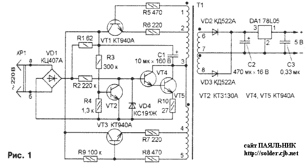
Rectified diode bridge VD1 is the voltage across the divider R1 R3R4 is supplied to the base transistor VT2, and through resistor R2 to the base of the composite transistor VT4, VT5. During each half cycle until the voltage at the connection point of the collectors VT1, VT3 relative to the emitter VT2 does not exceed 100 In, he closed and opened VT4VT5 and the capacitor C1 is charged through the resistors R1, R10 and plot the emitter-collector transistor VT5. When the voltage at the specified point above 100 V, VT2 opens and bypasses composite emitter junction of the transistor. Capacitor C1 is discharged, feeds the oscillator transistors VT1, VT3, assembled on the Roar (see the book Ivanov A. Tsyganova And Khandogin and V. I. "secondary Sources power microwave devices". - M.: Radio and communication, 1989).
The oscillation frequency oscillator - about 60 kHz. From the secondary winding of the transformer T1 voltage of about 7 V. It is rectified by diodes VD2, VD3, smoothed the capacitor C2 and stabilizes the integral stabilizer DA1. Capacitor NW reduces high frequency pulsations.
Maximum voltage collectoremitter transistors VT1, VT3 in the steady state is not exceeds 200 V, VT4 and VT5 - 210 V. the Maximum current of the transistor VT5 when indicated on the circuit component values and the static current transfer ratio base h21e transistors VT4, VT5, equal to 25, does not exceed 300 mA.
At the moment of switching voltage collector-emitter transistors VT4 and VT5 may exceed 300 V. the collector current VT5 - 0.5 A, will lead to their failure. To limit the collector current VT5 at this point (when using transistors VT4 and VT5 with a large coefficient h21e) serve resistor R10 and Zener diode VD4. To limit voltage collector-emitter composite transistor between the collector and emitter VT5 it is desirable to include varistor voltage of about 250 V.
When using unit to power a low power load (with rated current not exceeding 5…10 mA) the resistance of the resistors R6 and R7 is advisable to increase to 470 Ohms, and the capacitance capacitor With 1 to reduce to 2.2…4,7 UF (in this case, the block will be less warm and reliability will increase).
Except CTA (VT2), the device can use any transistor in this series, as well as series KT3102 or foreign production with similar characteristics (for example BCW60D). Transistors CTA interchangeable on CTA, BF469/PLP (VT1, VT3) or CTA, BF459 (VT4, VT5).
Capacitors C1, C2 - imported, you can use K50-35, NW - K10-17. Diodes VD2, VD3 - any small silicon with a valid direct current of at least 100 mA reverse voltage of not less than 20 V and an operating frequency of at least 150 kHz. Resistors R1-R3 1 -4, ICA or others with a working voltage of at least 350, and the rest C2-33, S2-23 MLT, ALT or the like.
The Transformer T1 wound on two stacked ferrite (2000NM) rings size CHH. Winding 1-2 and 4-5 contain 8 turns of PEV-1 0,1, 2-3, and 3-4 - 200 turns of the same wire, winding 6-7 and 7-8 - 14/22/28 turns sew-1 0,17 (respectively for output voltages 5/9/12). For winding and outer insulation is recommended to use Teflon tape or film PAT.
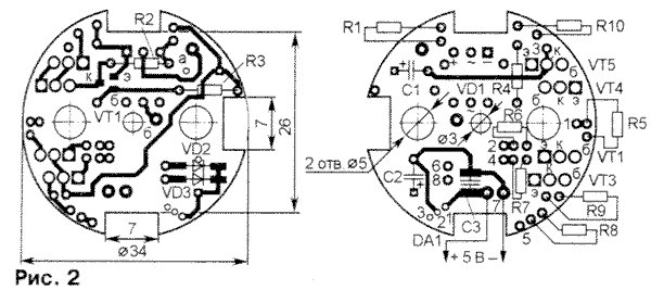
In the author's version of the power supply unit is mounted in standard plug with a diameter of 40 and a height of 27 mm. Printed circuit Board (Fig. 2) made of two-sided foil fiberglass thickness of 0.5 mm., the Distance between the centers of the holes in the Board under the pins of the plug 19mm. All resistors, except for R2 and R3, establish perpendicular to the Board. The Zener diode VD4 soldered to printed conductors with the installation of the transistor VT2. To the pads marked "a" and "b", solder the wires from the pins of the plug, and to the pads with figures 1-7 - the terminals of the windings of the transformer T1. Place it over the condenser NW in the free space between the transistors VT1, VT3 and the capacitor C2. Assembled from undamaged parts and without error in the mounting block does not require forging.
Author: A. Khabarov, Kovrov, Vladimir region; Publication: www.cxem.net