


")

Scientific and technological progress does not stand still, and radio-electronic devices devices become smaller, losing its volume and mass, and decreases current consumption. For certain devices, it helps to have a source power of a power not exceeding 400…500 mW or less. Power supplies on the basis of the low-frequency step-down transformers gradually replaced SMPS The only thing that has remained relevant to this day - galvanic isolation the load from the AC mains.
We offer SMPS is characterized in that simple to manufacture. Provides galvanic isolation of the load from the AC and withstands the output circuit. The disadvantages include low output stabilization voltage, but if necessary, this disadvantage can be eliminated by applying low-power integrated surge protector series 78Lхх or similar.
Specifications
- Supply voltage, .......220±10%
- Conversion frequency. kHz.......20 100
- Output voltage, V.......9…10,5
- Maximum output current, mA.......45
Diagram of the device shown in Fig. 1. Its basis is the chip IR2153D, which is a driver with a built-in generator. This chip is designed to control two series-connected the switching MOSFET and the building of a strong pulse voltage converters. Output stages of the driver is connected so that the power they received in parallel, whereby they operate as two half-bridge switch to the opposition. When connecting the pulse transformer to the outputs of these stages - and LO (pins 7 and 5) is it bridge circuit of the voltage Converter.
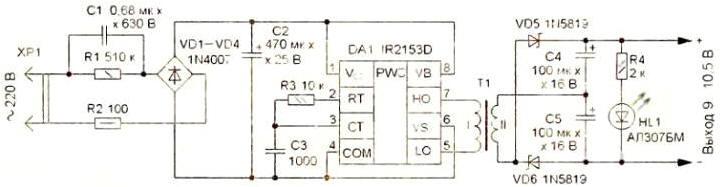
Fig. 1
It feeds the driver from the AC current through the quenching capacitor C1, current limiting resistor R2 and the rectifier diodes VD1 - VD4. Ripple smoothes the rectified voltage of the capacitor C2. The resistor R1 provides discharge of the capacitor C1 after disconnecting the power source from the mains.
Stabilization of power supply voltage is integrated Zener 15.6 V. conversion Frequency is set by the circuit R3C3, it can be defined by the formula:
F = 1/(1,4C3(R3+75 Ω))
When specified on the diagram the values of frequency conversion is about 70 kHz.
Output stages of the driver DA1 provide output switching current up to 200 mA. that allows you to connect the primary winding of the transformer T1 directly to the outputs of the chip. The AC voltage of the secondary winding supplied to rectifier voltage doubler, assembled diodes VD5, VD6 and the capacitors C4 and C5. About the presence of the output voltage is indicated by an led HL1.
In SMPS applied resistors MLT, C2-23, the capacitor C1 type K73-17 or imported, it needs to be designed to work with alternating voltage of At least 400, capacitor C3 - K10-17 or SMD, the remaining capacitors oxide domestic or imported. The 1N4007 diodes can be replaced by 1N4005, 1N4006 or low-power diode bridge, designed for use in 220 V, for example CCA. Schottky diodes 1N5819 interchangeable on 1N5817, 1N5818 or diodes series CD, KD521, KD522, but in the latter case, the output voltage will decrease by about 1 V. HL1 led can be any color of the glow.
The transformer is wound on a magnetic core size R10х6 x4 (EPCOS B64290L0038-N87) ferrite magnetic permeability 2200. Used the wire pelsho diameter of 0.12 mm. Primary winding is wound round in a row - it is about 85 turns (a tolerance of ±10 turns). To improve secure insulation of the primary winding of the cover 2…3 layers of lacquer, for these objectives applied aerosol automotive acrylic lacquer, which has high resistance to weather and mechanical influences. Then wound secondary winding 30 also turns round in a row.
Printed circuit Board for the device is not designed for All the details posted on prototype printed circuit Board with the use of wired installation (Fig. 2). Fee posted in plastic case dimensions 60-35-25 mm In housing need make holes for the led, network and output cables.
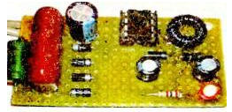
Fig. 2
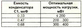
The output power of the power source depends on the damping capacity of the capacitor C1. The table shows its capacity for different values of output power.
Load characteristics of the source shown in Fig. 3.
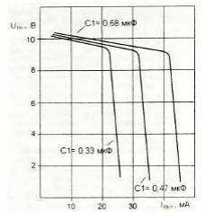
Fig. 3
If consumed load power is less than optimal, the excess energy will go into heating the of the chip. After Assembly, the device does not require any adjustment and can be immediately used to power the corresponding workload.
Author: A. Depalma