


")

The distinguishing feature of the proposed low-power switching power supply - a small number of parts and low cost. It is permissible to use for power a low power electronic equipment.
Specifications
- Input voltage, V......220
- Output voltage, V......5
- The maximum load current, And.....1,2
- Conversion frequency, kHz......50
Based on the miniature AC adapter (see article Tsypushtanov A. "Miniature network" in the "Radio" No. 4, 1986, p. 48). The device is made under the scheme half-bridge voltage Converter (see figure). One shoulder bridge form the capacitors C4 and C5, and the other transistors VT1 and VT2. In the diagonal the bridge includes the transformer T1.
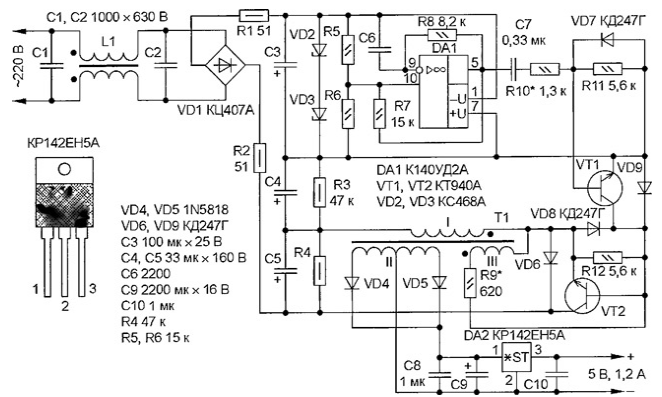
The generator at the shelter DA1 is built on a multivibrator. Voltage power stable Zener diodes VD2 and VD3. The oscillator frequency depends on the capacity of capacitor C6 and resistor R8, and to these in the scheme of values approximately 50 kHz.
Capacitor C7 provides isolated DC generator and transistor VT1. Resistor R10 limits the base current, and the diode VD7 - return the voltage at the emitter junction of transistor VT1.
One of the drawbacks of half-bridge Converter - the need for an additional transformer to control the transistors. The proposed the power source was able to solve this problem differently.
The opening of the transistor VT2 is happening in the moment, when a transistor VT1. The positive voltage feedback winding III of the transformer T1 is supplied to the emitter junction of transistor VT2, opening it. The base current transistor VT2 is limited by resistor R9. Return switching transistors occurs when opening the transistor VT1 pulse from the master oscillator and the shunting-emitter junction of transistor VT2 open diode VD8. In this moment through the transistors flows through the current, so to reduce it to the minimum should be selected resistors R10 and R9 to exclude deep the saturation of the transistors.
The output voltage from the winding II of the transformer T1 straighten diode VD4 and VD5. The rectified voltage is supplied to the stabilizer DA2. The Converter does not have node voltage and short circuit protection, so these the functions of the output linear voltage regulator DA2.
The device incorporates capacitors K73-11 (C1, C2).
The transformer T1 is wound on the annular magnetic ferrite CHH MNM. The primary winding has 300 turns of wire sew-2 0,2, secondary - 2x22-loop sew-2 0,5, winding III - 11 turns sew-2 is 0.2.
Establishing device is reduced to the selection of resistors R9, R10 for a specific the power value of the load based on the condition of saturation of the transistors VT1, VT2. For this oscilloscope via a voltage divider connected in parallel sections collector - emitter transistors. To start the selection with small values resistance, for example, R10 = 300 Ohm R9 = 100 Ω for maximum output power. Then increase the resistance until the beginning of the output transistor from the saturation. The measured resistance is reduced by half and set the resistor nearest suitable denomination. Under optimal selection of resistors the transistors are heated very slightly and it only needs to be installed on small heat sinks, an area of approximately 5 cm2 each.
The output voltage can be set by changing the number of windings II and applying the chip DA2 to the desired voltage.
Author: S. Gorshenin, Kazan