


")

In the present article describes a laboratory power supply, made on chips - voltage regulators. It contains two independent sources: a power with an output voltage from 1.25 to 27 and In maximum load current 3 A and a relatively low-power bipolar with voltage 0..±24 V and a current of 0.6 A.
Laboratory power supply unit (Fig. 1) consists of two independent sources A1 and A2, not galvanically connected with each other, and has a lot of opportunities.
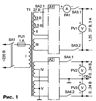
Main specifications
- The output voltage of the block A1.In......1,25-27
- The maximum load current (current limit) block A1, And......3
- The output of the bipolar voltage block A2, ......0…+24
- The maximum load current (current limit) unit A2,And......0,6
The device incorporates common to both sources of power transformer T1. Output voltage and load current more powerful source A1 can control using voltmeter and ammeter, which is made on the basis pointer device M2001. In the author's version output voltage A2 measure two identical digital voltmeter collected on the basis of ADC CREW. Schemes such devices have appeared on the pages of "Radio", for example, in the article [ 1 ], therefore, here to dwell on those not 'll.
Block A1 is a stabilizer, which is described in [2], performed on the local elements and revised by the author. Before a job is the possibility to regulate the intervals of the output voltage for the purpose reduction of losses in the regulating transistor. This unit can be used to power a variety of equipment and repair work, as well as charging device.
Power source A1 provides a stable output voltage in intervals of 1.25…6,5; 1,25 13…and 1.25 27…In, with the possibility of smooth adjustment. The maximum load current (trigger level on the supply voltage) can be set in the range of 0.05…3 A. In the case of exceeding level the unit automatically enters the constant current mode, and after the overload is removed is returned to the voltage.
The block diagram A1 shown in Fig. 2.
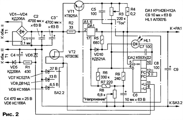
The device consists of the following functional parts: a power rectifier VD1-VD4 with filter C1-C3; the voltage regulator on a chip DA1 and the transistor VT1; node protection current OS DA2; two auxiliary sources stable voltage VD5VD6C4R1 and VT2VD7-VD9 to power OU DA2. Switch SA2 set desired interval of output voltage regulation.
If the load current does not exceed 50 mA, the device works as a stabilizer, included in the model scheme [3]. When the load current exceeds this value, the voltage drop across the resistor R2 opens the transistor VT1, thereby limiting the current through the chip DA1 at 50 mA. Regulate the output voltage variable resistor R8.
Node current power protection works as follows. Stable output voltage served on the non-inverting input of op-amp DA2. At its inverting input via adjustable divider R3R6 receives the amount of the output voltage and downs the voltage across current sense resistor R4.
Oh DA2 compares the stabilized output voltage with a voltage, coming from the divider, which depends on the load current. Until the voltage on the noninverting input is greater than the inverting, the output OS is installed a high level close to the output voltage. Diode VD10 and led HL1 closed. The device operates in the voltage regulator. If the current load increases, the voltage drop across current sense resistor R4 increases and at some point the voltage at the inputs of the opamps are equal. Thereafter, further increase of the load current occurs because the output of Oh shunt circuit adjustment of the stabilizer DA1 through open diode and VD10 led HL1. Resistor R5 limits the current through the led HL1 and Oh on an acceptable level. In this case, the voltage drop across the resistor R4 is supported constant due to the change of the output voltage at the load. Device goes into constant current mode, as evidenced by the steady light HL1. The restriction level of the load current is set by the variable resistor R3.
For normal operation of the device requires that the minimal difference input voltage (positive lead of the capacitor C3 and the output of the stabilizer pin 8 of the chip DA1) was not less than the minimum voltage drop chip DA1 and voltage open emitter junction of the transistor VT1 (in our case - 3.8).
The scheme of the bipolar voltage regulator A2 shown in Fig. 3.
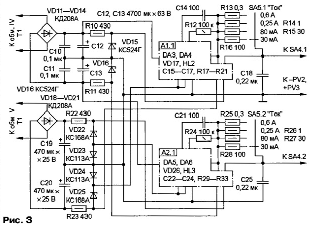
Dash-dotted line highlighted nodes A1.1 and A2.1 matching scheme with A1.1 Fig. 2. The Node A2.1 differs from A1.1 in that instead of CREA applied a voltage regulator negative polarity CREA [3] (he conclusion 8 - input, 2 - output, 17 - managing output), and diode VD26, led and HL3 the oxide capacitor C22 connected in reverse polarity.
The principle of operation of the device A2 is similar to the block A1 (see Fig. 2). The difference is that there is no strong control transistor, no the switch limits the output voltage and current adjustment actuation protection - stepped, with the switch SA5 and resistors R13-R16 and R25-R28. Current levels of fault - 0.6 A, 0.25 A, 80 mA and 30 mA - set in both channels simultaneously. Output voltage adjust from scratch through the provision of an offset voltage adjustment circuit stabilizers DA3 and DA5 separately in both channels. Regulate the voltage variable resistors R20 and R32 0 to +24 V and 0 to -24 V, respectively. Offset voltage remove from the support of a stabilized voltage source R22R23C19C20VD22-VD25.
Transistor CTA (VT1) it is permissible to replace any of this series. The transistor VT2 you need to pick up with the initial drain current of about 10 mA. Regulatory transistor (CTA) and integrated stabilizers mounted on a separate heat sinks or metal rear wall of the housing.
In the latter case, they should be securely insulated from the housing mica spacers. On the front panel rendered gauges, led indicators, controls, output terminals.
The size of the device depends mainly on the size of the mains transformer, the power of which should not be less than 180 watts. In the original network transformer - homemade, made in the tape toroidal magnetic core 120x60x32 mm from the voltage regulator for tube TVs. Primary (AC) coil contains 990 turns of wire PEL 0,4 - Winding II (for power block A1) contains 145 windings with taps on the 50th and 82nd turns of wire PEL with a diameter of 1 mm, the voltage across the terminals of the coil - 11, 18 and 32 with current less than 3.2 A. Winding III (support for block A1) consists of 45 turns wire PEL of 0.25. The voltage across winding - 10 V at a current of 20 mA. Winding IV (power to block A2) contains 256 turns of wire PEL 0,56 with a branch from mid. Voltage on it - 2x28 In with current 1 A. Winding V (support for block A2) consists of 110 turns of wire PEL 0.4 outlet from the middle. The voltage across winding - 2x12 at a current of 50 mA.
Correctly assembled device in adjustment not needed. You may need selection of individual instances of the OS. At desire it is possible to increase the output current sources in parallel the required number of regulatory elements transistors in parallel VT1 in box A1 (in the chain of emitters of the transistors should enable takavarasha resistors resistance of 0.1 Ohms) and stabilizers in parallel circuits, DA3, DA5 in block A2 (how to connect stabilizers in parallel, can be found in the article [4]). In this case it is necessary accordingly the resistance of the current sense resistors and, naturally, the use of more powerful mains transformer.
Laboratory power supply, in addition to its direct purpose, can perform additional functions and possibilities. Block A1 can be used as a charger in the device. The charging current is set by resistor R3 when closed weekends the terminals. The voltage at the battery (or battery) and the charging current control with a voltmeter PV1 and ammeter RA1, respectively.
With the help of block A2 can check out the p-n junctions of low-power semiconductor devices, capacitors of 0.1 µf and measure the voltage.
To test p-n junctions, switch SA5 choose the minimum allowable current. Resistor R20 (R32) establish a zero output voltage. By the weekend terminals "+" ("-") and "General." connected, for example, a diode and gradually increase the tension. If the diode is included in the forward direction indicator lights overcurrent HL2 (HL3). In this case, the voltmeter will show the value of direct the voltage drop across the diode. If the diode is connected in reverse direction, mode the operation of the power supply will not change. In case of inspection of the Zener diode in reverse turn on the voltmeter shows the voltage stabilization.
When checking the capacitors switch SA5 also choose the minimum current load. Resistor R20 (R32) set the maximum, but not more rated for a specific capacitor, the voltage at the output. By the weekend terminals (polarity of the oxide capacitors) connect a capacitor and include the switch SA4. On the flash duration of the overload indicator can to indirectly estimate the capacitance of the capacitor or to detect its leakage.
To measure the voltage at carrying out various experiments and repair the works you can use voltmeters block. Before work should be disabled the appliance from the power supply, Razumkov contacts of the switch SA4. The voltage the investigated device conveniently serve with block A1.
Literature
Author: A. Ants, Ryazan region POS.