


")

In order not to discharge the battery of the receiver when using the system protection, while at home, it connects to the stationary network source.
Diagram, Fig. 2.71 controls the condition of the batteries and, if necessary, automatically performs their recharge. In addition, in the case of the signal the transistor VT1 alarm performs amplification of the volume of the audio signal alert that provides ease of use. Indicator turning on the power supply to the network is the green glow led (HL1), and when the charge mode of the battery glows red (HL2).
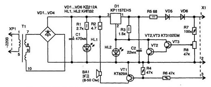
Fig. 2.71. The circuit of the power source with charger
The device operates as follows.
Chip D1 performs the stabilization of the output voltage, the level of which maybe a step change (6,6 or 5 - it depends on the led glows HL2 or not).
Led HL2 except light indication of the charge process is also a source the reference voltage 1.6 V for the chip.
Transistors VT2 and VT3 assembled analyzer level output voltage the power source. Due to the large gain of these transistors they switched from a locked position to an open position when the voltage on the output of 0.1 V.
The scheme is connected, the battery is configured by the resistor R8 so that the threshold of opening of transistors was approximately 3,9…4 In (with LEDs HL2 should be off). The magnitude of the current through the batteries depends on their condition, and as you charge it gradually decreasing. The maximum charge current is limited to about 20 mA (set the value of the resistor R5).
As you grow capacity charge voltage on the battery is gradually increasing, and, when it reaches the value of 3.9 V, the output voltage D1 reduced from 6.6 V to 5 V. In this case, the charging will stop.
The circuit has fixed resistors MLT, rigged R8 type SP5-2; electrolytic capacitors C50-35 25 V. the Diodes can be replaced at any a current of at least 500 mA reverse voltage 50 V.
The LEDs used different colors from the series. CHIP or similar with small quiescent current when the glow. The transformer is suitable from unified, for example type TN-220-50, or any other voltage in the secondary winding 9…12 V
Version of the PCB layout and the location of elements in the source schema supply is shown in Fig. 2.72.
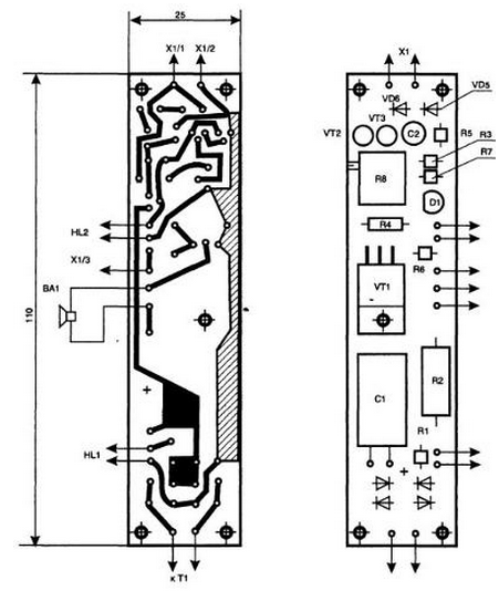
Fig. 2.72. A printed circuit Board, and the location of elements on the schema power source
Structurally, the power supply housing is in the form of coasters the receiver, but in this case a vertically mounted receiver connected through the corresponding socket connector (X1) to the circuits of the power supply. Connector X1 applied type MRN.
Author: I. P. Shelestov