


")

Describe unusual rectifier AC is designed for use where required small adjustable voltages at relatively high currents and low losses. Example the application can serve as the power to the Peltier elements used in the systems cooling, where, in addition, it is necessary to adjust the temperature. The plating bath and the low-voltage soldering irons - other application examples such rectifier.
When you receive a low supply voltages the rectifiers have the problem of the voltage drop across rectifier semiconductor diodes, due to applied to the semiconductor diodes material (0,9 0,6…in silicon diodes), which has the greater the impact of the lower rectified voltage. There is a problem of heat removal during large load currents. When necessary, the adjustment of the output voltage, use a consistent voltage stabilizer, drop the voltage at the transition of the regulating transistor which is in addition to the drop on the diodes of the rectifier are still a few volts, which leads to useless power dissipation, efficiency of the device, thus, does not exceed 50%. In the picture (Bild 1) shows a diagram of the rectifier is taken from the collection of patents GDR [ 1 ], which can significantly reduce power loss.
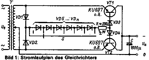
Fig. 1.
It is, primarily, about the full-wave rectifier with an average point, which is typical and famous as rectifier with two diodes and a branch of the middle winding of the transformer. Here, the rectifier diodes are replaced by transitions emitter-collector regulatory transistors (VT1 and VT2). This provides an advantage over the diodes, so as the voltage drop at the junctions of the emitter-collector of the modern powerful planar transistors is only 0.1…0.2 V, from about 0.7 V at most rectifier diodes, therefore, useless power dissipation znachitelno reduced. In addition, when using transistors as managed elements, it becomes possible to adjust the output the rectified voltage, and, specifically, by phase truncation.
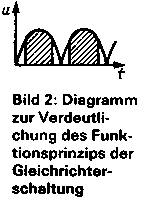
Fig. 2
During the positive half cycle current flows through VD1, the contacts of the switch S (S - first to the right, the diagram position), resistor R and diode VD4 circuit, the base-emitter VT2. VT2, wherein, managed, resulting in the lower branch of the rectifier is open, and the capacitor C is charged. During the negative half-period of the transistor VT1 is managed through the diode VD2, S, R, and VD3 than the upper branch opens the rectifier. Since this is a full-wave rectifier in which the residual voltage drop at the junctions of the emitter-collector transistors very small, small and dissipated in the transistors power equal to the voltage drop the emitter-collector multiplied by the current flowing in this circuit. Col low power dissipation, may be small and the heat sink, and if the negative pole of the rectifier may be connected with metal housing the powered device, the regulating transistors can be screwed conclusions collectors directly to the chassis without the insulating strips.
Now consider the ability to adjust the output voltage of the rectifier with a chain diodes VD5…VDn dial switch S engaged shutoff phase (Bild 2). Transistors, in this case, start not from the beginning of the the corresponding half cycle of the AC voltage, and after a while, when the instantaneous amplitude of the voltage at halftime exceed the amount of direct voltage connected diodes. Accordingly, the less time opened transistors, the to a lower voltage to charge the filter capacitor C. Of course the effect of the later opening and earlier closing of transistors depends on the direct voltage drop across the diodes VD1…and VD4 of the voltage opening of transistors VT1 and VT2. It is best to use germanium diodes because of the small direct voltage drop on them, for example, 0.1 A or 1 A diodes from series GY. More modern here are diodes with Schottky barrier, but the results obtained with them no better, but worse than with good old germanium diodes, the more that is still not all can Schottky diodes to get.
You should pay special attention to the maximum allowable reverse voltage transitions, the base-emitter VT1 and VT2. If you exceed this voltage, the current from the corresponding outer end of the secondary winding of the power transformer will flow through the locked emitter-base (as current stabilization (or "avalanche breakdown current") in the Zener diode) and thence through included in the forward direction of passage of current to the base - collector, - right at the rectifier output. In this case, of course, about any regulation the transistors can not be and speeches and they are damaged. The peak value voltage on any half of the secondary winding must not exceed the allowable reverse voltage emitter-base (Ueff * 3 2), which must be in within 6…9 V.
It is recommended to install the transistors in the circuit to measure permissible reverse voltage transitions, the base-emitter (and, probably, since the scheme symmetric, pick up a pair of transistors with the same parameters). Method measure this voltage is simple: you must include the junction between the base and the emitter in return (locking direction to the passage of direct current through the resistor and measured transition voltage just as is determined by the voltage the stabilization of the conventional Zener diode. Increasing the voltage applied to series resistor (for example, a resistance of 1 kω) and the transition base-emitter ("plus" to the emitter, if it is n-p-n transistor) in parallel the transition included the voltmeter observed value of the maximum reverse voltage, when it ceases to grow significantly with increasing voltage power. The latter circumstance (rather low return valid the voltage of the junction, the base-emitter) limits the maximum output voltage driven rectifier circuit 5 volts. The resistance value R = 200 ohms selected as a compromise for the output voltage to 5 V load current 1…2 A: too small a value leads to unnecessary losses in the resistor (uneconomical), large, does not allow the full opening of the transistors, what also increased losses (now on regulatory the transistors).
The transistors must have as more permissible reverse voltage of the junction, the base-emitter and possess the maximum possible gain current. If we apply p-n-p transistors (for example, CT), all the oxide diodes and a filter capacitor needs to be "flipped" and the polarity of the output voltage will change.
You can go ahead and instead of discrete adjust the output voltage to apply a smooth, setting instead of diodes VD5…VDn and switch S, of the same conductivity as VT1/VT2 (collector-to-point connection of diodes VD1 and VD2, the emitter to resistor R and potentiometer, the output the engine which should be connected with the base of the additional transistor, and the extreme conclusions - with the collector and emitter of this transistor. There are also other inclusion with falling characteristic (similar to the dynistor). For the experimenter here is a great field.
Literature
Translation: Victor Besedin (UA9LAQ) This email address is being protected from spambots. You must have JavaScript enabled to view it. , Tyumen; Publication: www.cxem.net