


")

In the published article here our writer analyzes the circuitry of antenna amplifiers Polish production and justifies their conscious approach to their choice from the point of view of noise coefficients and gain. It also makes recommendations for the repair of such devices, quite often out of order from lightning discharges, and elimination of self-excitation. This will allow/ I hope many hams not only to select the amplifier, but also to improve its performance.
Active antenna Polish company ANPREL and some other widespread in Russia and CIS countries. With little own gain, especially in the range of MB, the parameters of this antenna are largely determined by built-in antenna amplifier. It is this block a number of inherent weaknesses: he is prone to delays, has a fairly high noise level, easily overloaded strong signals of MB range, are often damaged by lightning discharges. These problems are familiar to many owners of such antennas.
The operation of antenna amplifiers SWA and similar very little covered in the literature. One can only note the publication [1], which indicates an overload of the amplifier from MB. Other disadvantages to the owners of the antennas has to fight a known manner: replacing amplifiers, choose the best. However, this method requires much time and effort, since the amplifier is typically hard to reach - located with the antenna on a high mast.
Based on the analysis circuitry, own experience and some materials firm ANPREL, offer a more informed approach to the selection of amplifiers, the method of repair that allows you to recover the corrupted block, and in some cases to improve its parameters.
The market is filled with many interchangeable models of antenna amplifiers manufactured by the firms ANPREL, TELTAD, etc. under different trademarks and rooms. Despite this diversity, most of them collected by the standard procedure and represent aperiodic two-stage amplifier bipolar microwave transistors included in the circuit with the MA. In confirmation of this we will consider models of different companies: the simple amplifier SWA-36 firms TELTAD, schematic diagram of which is shown in Fig. 1, and a common amplifier SWA-49 (analogue SWA-9) firms ANPREL - Fig.2.
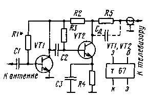
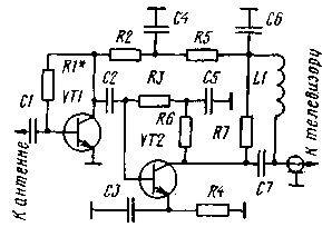
Fig.1-2
Amplifier SWA-36 contains two broadband gain stages on transistors VT1 and VT2. The signal from the antenna via a matching transformer (not shown) and the capacitor C1 is supplied to the base of transistor VT1, connected in the circuit with the MA. The working point of the transistor is set by the bias voltage determined by the resistor R1. The current negative feedback (EP) linearizes the voltage characteristic of the first stage, stabilize the working point, but slightly reduces its gain. The frequency correction in the first stage is missing.
The second stage also performed on the transistor on the circuit with the MA and EP voltage through resistors R2 and R3, but has a current EP via the resistor R4 in the emitter circuit, rigidly stabilizing mode of the transistor VT2. In order to avoid large losses gain resistor R4 is shunted AC condenser NW whose capacitance is chosen relatively small (10 pF). As a result of the low frequency range of the capacitive resistance of the capacitor Sz is a significant and emerging environmental AC reduces the gain, thereby correcting the frequency response of the amplifier.
The disadvantages of the amplifier SWA-36 may include passive losses in the output circuit of the resistor R5, which is included so that it falls as a constant voltage and the signal voltage.
Similarly constructed amplifier SWA-49 (Fig. 2), which also has two cascades, collected under the scheme with the MA. It differs from SWA-36 best isolation of power circuits using l-shaped filters L1C6, R5C4 and high gain due to the presence of the capacitor C5 in the chain EP (R3C5R6) of the second stage and transitional capacitor C7 to the output.
Such circuitry inherent to most other amplifiers SWA (see, for example, the amplifier circuit SWA-3, depicted in [1]). Minor differences are most often in the second cascade, which may be provided with different frequency correction circuits, available in various feedback and consequently the gain. Some models, such as SWA-7, the first and second stages have a direct link to the output collector of the transistor VT1 is connected directly with the withdrawal of the base of the transistor VT2. This allows you to cover both the cascade loop of EA DC and thereby improve the thermal stability of the amplifier.
In the cascade transistors connected in the circuit with the MA, the most important of the internal connections and tanks transitions of transistors. It manifests itself in limiting the bandwidth and the tendency of the amplifier to the excitation, the probability of which is greater, the higher the gain. For its evaluation it is known the concept of tolerance - limit values of gain, above which the amplifier becomes an oscillator. Many antenna amplifiers SWA with a high gain are at the threshold of stability, which explains their frequent self-excitation.
As measures to improve the stability of amplifiers firm ANPREL it uses a separate circuit (affecting the capacity of the installation), surface and volume coils, chokes, etc. a More radical way: the inclusion of transistors on cascadei the circuit with the MA-ABOUT - why-that is not used. At constant switching circuit of the transistors MA-MA to solve sustainability of the firm prefers to produce regulated power supplies. Decrease its voltage cannot fix the self-excitation of the amplifier while maintaining sufficient gain.
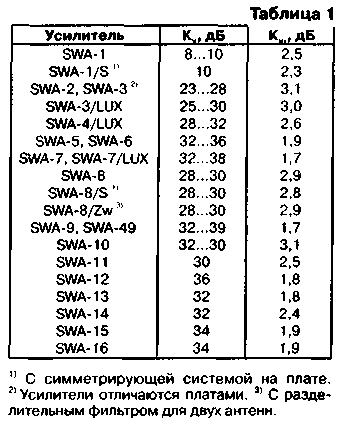
The main parameters (noise figure of Cs and the gain Ku) base models SWA company catalogue ANPREL are listed in table. 1.
Consider the interrelation of the basic parameters with the circuitry of amplifiers and their impact on the quality of reception.
As is known, the gain at high frequencies in the cascades with the MA critical parameters of the used transistors, especially to the cutoff frequency frp. Amplifiers SWA, applied to the bipolar microwave transistors of the structure n-p-n, marked as T-67, at least - 415, which determine the maximum achievable gain Ku a two-stage amplifier of about 40 dB. Of course, working in such a broad band of frequencies the gain is not constant - it changes reach 10… 15 dB due to the uneven frequency response at the highest frequencies of the range, and the correction to the lowest. Maximum gain Ku is difficult to ensure the stability of the amplifiers, so in some models it is limited to values up to 10…30 dB, which in many cases is sufficient (see tab. 1).
Contrary to popular belief, it should be noted that the gain cannot be considered as the main parameter of the antenna amplifier. Because TVs themselves have a very large stock of their own gain, i.e., Have high sensitivity, limited amplification. Worse they have a sensitivity limited by synchronization. Finally, the lowest sensitivity is limited by noise [2]. Consequently, the determinant of distant reception, you should take the noise floor of the electronic tract, and not the gain. In other words, restriction of intake primarily occurs due to the influence of noise interference and not due to the lack of signal amplification.
The effect of noise is estimated in relation signal/noise, the minimum value of which was equal to 20 [2]. In this regard, and determine the sensitivity, limited by noise, which is equal to the voltage of the input signal is 20 times higher voltage noise.
For TVs the third to fifth generations, the sensitivity is limited by noise, is $ 50… 100 µv. However, when the ratio signal/noise ratio equal to 20, there are very bad image quality and clarity only the major details. To obtain a good quality image should be submitted to the television input useful signal, is about 5 times greater, thus improving the signal-to-noise ratio of about 100 [2].
Antenna amplifier to increase the signal-to-noise, and amplifying the signal, not noise. But any electronic amplifier inevitably has its own noises, which are amplified along with the desired signal and degrade the signal-to-noise ratio. Therefore, the most important parameter of the antenna amplifier should be considered as the noise coefficient Ksh. If he is not small, the increase of the gain is useless, because both the signal and the noise are amplified equally and their attitude improves. As a result, even when a sufficient signal level at the antenna input on the TV the image will be amazed by the intense noise nuisance (well-known "snow").
For a single estimate of the noise multistage tract there is a figure given to the input of the noise figure of Cs, which is equal to the noise at the output divided by the total gain, i.e., CABG=coronary artery bypass grafting.o/Ku. Since the output level of the noise Cs.o depends to the greatest extent from the noise of the first transistor, amplified by all subsequent stages, the noise remaining stages can be neglected. Then CABG.o=CSCO, where Cs, is the noise factor of the first transistor. Therefore, get Sh=KS, i.e. shows the noise figure of the amplification path is independent of the number of stages and the total gain is equal only to the noise factor of the first transistor.
This implies an important practical conclusion - the use of antenna amplifier can give a positive result when the noise factor of the first transistor of the amplifier is less than the noise figure of the first stage of the TV. In selectors, channels TV fifth generation of the FET transistor KPA with a noise figure of 4.5 dB at 800 MHz [H]. Therefore, in the first stage antenna amplifier needs to operate the transistor with X<4.5 dB at the same frequency. Moreover, the smaller this value is compared with the coefficient X the TV, the more efficient use of the amplifier and the higher the quality of reception.
The noise factor also depends on the quality of matching at the input of the amplifier and the mode of operation of the first transistor. For amplifiers SWA type transistor VT1, the mode of its operation and the quality of the negotiation determines the given coefficient Cs= 1.7 to 3.1 dB…(see tab. 1).
From the above it is clear that the choice of the antenna amplifier on the principle - the more gain, the better is wrong. That is why many owners, changing amps, can't get a good result. The reason for this paradoxical, at first glance, the fact is that the noise factor is usually unknown (it is not in trading information firms), and he's actually slightly different on many models with different amplification (see tab. 1). The increase of the gain at a constant noise factor does not give a gain in signal-to-noise and thus improve the reception quality. Rare success is only achieved when accidentally comes across a low-noise amplifier.
Therefore, when selecting antenna amplifier should focus primarily on the minimum noise level. Quite good can be considered an amplifier with CABG<2 dB. From table 1 can be considered the best model SWA-7, SWA-9 having CABG=1,7 dB. Information on the noise figure of the new amplifiers can be found in the directory of the company ANPREL or on the Internet.
As for gain, it is, of course, is also important, but not for the maximum amplification of weak signals, and, primarily, to compensate for losses in the connecting cable matching the splitter devices, etc. due to these losses with insufficient amplification of the signal level at the input of the TV may fall below the threshold, limited sync or even gain, which will make reception impossible. Therefore, for a proper choice of gain is necessary to know the attenuation of the signal in all connective tract. And its estimated value is easy to calculate.
Linear attenuation of the signal in the distributed cable RK brand-75-4-11 equal to 0.07 dB/m at the first-fifth, of 0.13 dB/m at the sixth-and twelfth of 0.25…of 0.37 dB/m at 21-60-m channels [2]. When the length of the feeder 50 m attenuation at 21-60-m channels will be 12.5…of 17.5 dB. If there is industrial passive splitter, it introduces additional losses at each of its output, the value of which, as a rule, is indicated on the body.
Calculating the attenuation in the cable and instead of the attenuation in the splitter (if any) that receive the minimum gain of the antenna amplifier. To it add the stock in 12…14 dB to amplify weak signals, which is necessary due to the low efficiency compact broadband receiving antennas. According to the obtained value of RL is chosen antenna amplifier. Far exceed the obtained value of the gain does not follow, as it increases the likelihood of self-excitation and overload strong signals closely spaced stations.
Repair of antenna amplifiers is largely confined to the active replacement of items damaged by lightning discharges. It should be noted that in some models of the diode at the input does not guarantee a complete lightning protection: when a powerful atmospheric discharge makes its way as a protective diode, and as a rule, both transistors.
Antenna amplifiers SWA collected by the technology of automatic surface Assembly micronutrients that requires accuracy in the repair. Soldering should be performed small soldering iron with a sharp sting. Idle amplifier carefully, trying not to damage the delicate traces, unsolder microdentistry VT1, VT2 and protective diode (if any).
The main parameters of the domestic transistors, suitable for installation in amplifiers SWA, are listed in table. 2 [W]. From this it follows that the use in the first cascade transistors CTA-2, CHA-2, CHA-2, CTB-2, CTV-2 noise performance of most amplifiers is not worsen, and the use of transistors TA-2, TB-2, TB-2, CHA-2 CABG reduces to 1.5 dB, which improves the parameters of the amplifier. This allows us to recommend the replacement of the first transistor of the amplifier for these last even in good, but "noisy" amplifiers, with the aim of improving the quality of their work. It should be noted that in table. 2 shows the limit values of the model parameters, as a rule, the better [W].
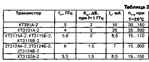
Low-noise microwave transistors series T, KT relatively expensive and low voltage, so it is better to only install in the first stage and the second to use cheaper and more powerful transistors CTA-2, CHA-2 (see tab. 2) and even series CT, CT, CT,CT and others with a cutoff frequency of about 2 GHz [W]. However, in the latter case will be slightly less gain at the upper frequency range.
Case dimensions import microtransaction equal to 1,2x2,8 mm length of pins 1…1.5 mm. Respectively, and the distances between the printed circuit Board pads to terminals of transistors is small. The unit produced transistors with a diameter of 2 mm from the mounting surface, though possible, but difficult: when soldering them can be corrupt. New transistors better to install from the opposite side of the Board, pre-drilled holes for the pins in a drill with a diameter of 0.5…0.8 mm. it is Better to drill not in the printed guide, but the hole touched the edge of the site. If on the side opposite to the surface mounting, a foil layer, the holes in it should be time-countersink drill bit with a diameter of 2…2.5 mm (except the holes for the output emitter of the transistor VT1).
Then install new transistors so that crystallochemical or the housing of the device concerned Board. If the findings are significantly on the other hand, after soldering them to bite. Microwave transistors are sensitive to static electricity, so when soldering it is necessary to comply with the relevant protection measures. The soldering time not over 3 with [H].
The protective diode can not install. The best protection against atmospheric electricity serves as a good grounding of the antenna.
Amplifiers SWA both transistors operate with a collector current of 10 to 12 mA. After replacing this current is acceptable for the second transistor (for example, CTA-2), but constantly exceed the allowable for the first, if the transistors of the series CT, CT and CTA-2 (see tab. 2). Collector current depends on the parameter h21e, whereby the transistors have significant scatter. Therefore, after mounting a particular instance it is necessary to set the operating point of the transistor VT1. To do this, the fed microreactor R1 and instead, temporarily connect a trimmer (SDR-23, SDR-27, etc.) resistance 68…100 kOhm. Before turning on the power engine of the resistor should be in the position of maximum resistance, to prevent damage to the transistor.
The amplifier serves voltage of 12 8 from the power supply and measure the voltage drop across the resistor R2 (see Fig. 1 and 2). Dividing the measured voltage by the resistance of the resistor R2, learn collector current. Adjusting the resistance trimmer downward, making the collector current of about 5 mA, which corresponds to the minimum noise characterization of transistors [H]. In this setting finish and instead solder a trimmer same constant resistance (MLT-0,125 or imported) by shortening the pre to the minimum of its conclusions.
After that, cover the printed circuit Board and a planar transistor radio layer of varnish or compound. Appearance restored amplifier SWA-36 shown in Fig. 3. It uses transistors (Fig. 3,a) TB-2 (VT1) and CTA-2 (VT2). In connection with the simplest design of the amplifier is taken to eliminate self-excitation: the output collector of the transistor VT1 wearing ferrite microcalc (it is used in the channel selectors SC-M TVs ZUSTST and USCT). The collector current of the transistor VT1 is set by resistor R1 (Fig. 3,6) value of 51 ohms (33 ohms).
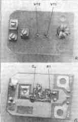
Fig.3
In the second cascade transistors were tested series CT, CT, which was maintained stability and sufficient gain. When this was checked the extra DM capacitor capacitance 150 pF (Fig. 3,6), a shunt resistor R5 (see Fig. 1) to increase gain. When installing the capacitor self-excitation of the amplifier may be reduced by lowering the supply voltage.
In the basic version (with transistors TB-2 and CTA-2) amplifier provided better than before the repair, the reception quality which is visually evaluated about the same reception with a new amplifier SWA-9.
Literature
Author: A. Pakhomov, Zernograd, Rostov region; Publication: N. Bolshakov, rf.atnn.ru