


")

The author's device is designed for automatic feeding bells in schools and other educational institutions in accordance with the applicable the moment class schedule. Unlike described in the time programmer training time ("Radio", 1985, No. 11, pp. 30,31) it eliminates the need for daily enable, allow short the voltage is switched off without interrupting the operation, provides the opportunity select any one of four pre-set programmes submission calls. Different device and a simpler circuit decision.
Schematic diagram of the programmer shown in Fig. 1. It consists of shaper minute pulses (DD1). divider, forming of them pulses with period of 5 min (DD2.1, DD3.1-DD3.3). calculating a logical block (DD2.2 and DD4-DD7). EPROM (DD8) and the node ring (DD9. \/T1 \/S1).

Works programmer. Pulses with a duration of 1 min from exit 10 of the chip DD1 fed to the divider, and with him (vyv. 5 DD2.1) pulses with a period of 5 min (4 min duration logic zero and 1 min - logical units) enter the input calculating a logical block, which outputs (pin. 2, 4, 6,10,12, 15 DD6 and 2. 4 DD7) connected to address inputs of EPROM DD8. Every 4 and 1 min for 10 h 40 min information on these inputs will change alternately from 0 to 255 in the binary system. This time is sufficient for submission calls shift operation of the school. Within just a specified time at the outputs 6 and 11 chips DD4 will be a logic level zero, which, passing through the elements DD3.4, DD7 and DD9.1, reaches input sample V2 EPROM DD8. On the same outputs of this chip in accordance with the recorded program or appear logical zeros or logical units. The call is activated when the outputs DD8 there is a logical unit.
It happens this way. Because at the outputs 6, 11 ICS DD4 there is, as mentioned above, a logic level zero, then the same voltage and 4 inputs. 5 element DD9.2 chips DD9. So on inputs 9. 10 item DD9.3 will be at this time, the levels of the logical units on it the outlet 8 is a logic level zero, and the output element 11 DD9.4 - level logical units.
As a result will begin charging the capacitor C10 and through the winding of relay K1 will flow current. The relay will go off and the contacts to close the circuit between the control electrode and the anode of the triac VS1. which will include the call. When the output 6 or 11 chip DD4 appears the level of logical units, the same level installed at the inlet of the sample EPROM \/2 and the inputs 4, 5 of the element DD9.2. Therefore, the output 6 of this element and the output element 11 DD9.4 to present a logic level zero. In this position, the capacitor C10 you cannot charge, the current through the relay coil K1 will not flow and the bell will ring.
A day after the inclusion of programming at the outputs 4 and 11 chips DD4. and consequently, at the output 11 of the chip DD5 appears logical unit, and reset the counters to zero state. As a result, the programmer will automatically resume its work. The installation of meters in the zero state in the moment you turn the programmer to the network element DD5.1 To increase the load capacity of the CMOS chips their outputs connected to the inputs Hook up circuits through transducers levels.
Schematic diagram of power supply programmer training time shown in Fig. 2. Before you switch on the machine switch A (Fig. 1) select the desired the program flow of calls, and then in the moment of doing, for example, at exactly 8 h 30 min. consistently include switches and ZA2 ZA1 (Fig. 2). At this point the bell rings signaling the beginning of classes.
Turn the machine on weekends and during summer vacation switch SА1 (Fig. 2).
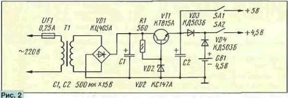
The details of the programmer is recommended to mount on the Board of foil fiberglass. The power bus, it is desirable to etch, and the remaining connections to perform thin stranded wire. Capacitors C5-C8 should be evenly across the power rails of the chip.
When installing used fixed resistors MLT-0,125, oxide capacitor programmer C10 - C50-16. and the remaining km. Quartz resonator ZQ1 - on the frequency of 32 768 Hz.
Chip KIE can be replaced by CIE, CRRT - CRRT. and 555 - similar series K155, 531. Relay K1 is any voltage positives In about 4 and a trip current of 30 mA. At higher current triggering transistor KT315B (see Fig. 1) you need to replace more powerful for example, CT, CT with any letter index. It is also desirable that the relay contacts were rated for a voltage of 220 V. In the original the programmer applied the relay RASA (passport 4.569.724).
Transformer power supply must have a capacity of not less than 5 watts and the voltage at the secondary winding 7…9 V. the Transistor VT1 (Fig. 2) should be installed on a heat sink. Instead KTA suitable CT, KT807 with any letter index. Capacitors C1-C2 - C50-6. As a switch A (see Fig. 1) and switches SА1. SА2 (Fig. 2) you can use any available. It is important only that they were located in a convenient location. The device itself should put in a small case and hang it on the wall next to the call button.
The establishment of the programmer is to install the required duration call selection of capacitor C10.
In conclusion, let us dwell on the EPROM programming CRRT. Circuits devices programming circuits have also been repeatedly documented (1-3). There's also a detailed description of the programming process.
Need a code address in accordance with the schedule in which the EPROM write a logical 1 can be found by the formula:
A(n) =(T(n)-T(0))1/2.5,
where A(n) - address code in the decimal number system (n=1,2…); T(0) - the start of classes, min; T(n) - ring, min.
Explain how to use this formula for a specific feeding schedule calls:
8: 30 - 9 hrs 15 mins - 1st hour, first shift;
9 h 15 min - 9 h 20 min - change:
9 h 20 min - 10 h 05 min - 2nd lesson, first shift, etc.
18 h 15 min - 19 h 00 min - 6th lesson, the second shift.
In this case
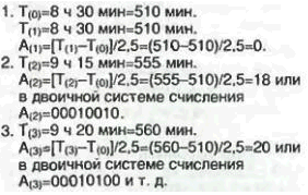
Therefore, in EPROM on the output, for example Q1, you need to write logic 1. when the address inputs set code: 0000000. 00010010 (i.e., at address the entrance of the JSC must be logic 0, A1 - 1. A2 - 0. AZ - 0. A4 - 1. A5 - 0. A6 - 0. A7 - 0). 00010100 (i.e., the address inputs AO must be logic 0. A1-0.A2-1,AZ-0.A4-1.A5-0.A6-0. A7 - 0), etc. the other Three feeding schedule calls can be recorded on the outputs Q2-Q4.
Literature
Author: A. Koutouzov, Atyrau, Kazakhstan