


")

In the national economy is widely used equipment powered from three-phase network requiring observance of the phase sequence. Usually this is achieved the corresponding switching wires, but during various renovations when use additional power cables or temporary distribution shields, switching is often a violation of the sequence of phases, which can cause the failure of the equipment.
The proposed device (Fig.1) ensures the correct sequence of the phases on the load randomly its connection to three-phase network.
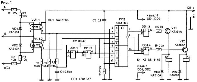
Works automatic switch phases. Negative half wave a sinusoidal voltage of phase A passes through the diode VD1 and creates the voltage drop of about 0.7 V. the Led of the optocoupler VU1.1 is not lit, so as to it is applied reverse voltage, the phototransistor of the optocoupler is closed. Positive half wave sinusoidal voltage of phase A passes through the led of the optocoupler VU1.1 and causes it to fluoresce. The phototransistor of the optocoupler VU1.1 is opened, and the emitter (pin 8) you receive the high voltage level. Pulse width the emitter is practically corresponds to the duration of the half cycle of the input signal.
Negative half wave of the phase In (C) passes through the diode VD2. led coupler VU1.2 is not illuminated and therefore at pin 5 is low. When positive half-wave current flows through the led VU1.2, the transistor of the optocoupler is open, and pin 5 VU1.2 - high level which is fed to the clock inputs of the flip-flop DD2. Diodes VD1, VD2 are needed to eliminate the high reverse voltage the LEDs of the optocouplers VU1.1 and VU1.2.
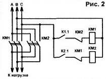
The output signal from the optocoupler VU1.1 is supplied to the information input of the upper trigger DD2 and integrating chain R7-C1. Heartbeats set both triggers in the States corresponding levels on the informational inputs in these time points. State change triggers occur on the fronts clock pulses (the transitions 0 - 1 ). Thus, the direct output (the output 1) upper circuit trigger DD2 - state "1" (high level), if the resistor R3 is connected to the phase b, and "0" (low level) when it is connected to the phase C. Phase connected to the resistor R1, is always taken for phase A. This information is sufficient to correctly connect the load to the network. Scheme control actuators is shown in Fig.2.
Signals with direct and inverse outputs of the upper trigger is received on the inputs logic elements DD1.3 and DD1.4 (Fig.1). Second inputs of these elements connected to the direct output of the lower flip-flop DD2. Logic element DD1.1 together with the integrating chain R7-C1 performs the delay of the signal at the time of inclusion device. The elements DD1.1, DD1.2, together with capacitor C2 form a trigger Schmitt, which produces signals with steep fronts.
Low the output DD1.1 occurs when at its inputs is "1". This happens when the voltage on capacitor C1 exceeds half of the supply. When indicated on the diagram the values of R7 and C1 of "1" appears in the information input D lower trigger DD2 approximately 1 second after the voltage on switch. Endurance is necessary to prevent intermittent inclusions load, for example, in case of unreliable contacts or arcing that often if there is a temporary network connections. At short-term shutdown network OPTRON VU1.1 not working, resistors R5 R7… - "0" and the capacitor C1 quickly discharged through the resistors R6, R7. This leads to a "0" on information input (pin 9) of the lower flip-flop DD2, which is transmitted to the trigger output (pin 13). Consequently, the outputs of the elements DD1.3 and DD1.4 set to "1". transistors VT1. VT2 is closed and both turnips - K1 and K2 - go. Consequently, the load is de-energized.
With the resumption of power supply time delay is repeated. The Chain R8-C3 sets both flip-flop to its original state at power-up. When normal operation of the low level switch will only appear on one output elements DD1.3 or DD1.4. The simultaneous appearance of a low level at their outputs excluded, because they are driven by anti-phase signals from the top of the trigger DD2.
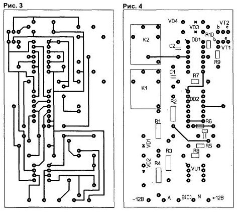
The device is assembled on a double sided printed circuit Board, the drawing of which the arrangement of elements shown and Fig.3 and 4.
Literature
Authors: V. Kalashnik, N. Cheremisinoff, Voronezh