


")

Modern TVs can be switched off after a certain, a user-specified time or at the end of TV shows ("SLEEP"). About makeshift timer that provides that functionality, is described in published here article. It can be used in the TVs are older models.
Currently released imported TVs equipped with very various user functions. One, and very convenient, the function you can read the SLEEP mode ("sleep"), allowing the user on their own the desire to choose the time interval after which the TV switches to duty mode. It is also worth noting a feature called AUTO SLEEP, when which the device turns off when you shut down the channel.
In our country operated a large fleet of TVs of the early issues, in lacking many service functions. For review the radio device is intended to equip an old machine SLEEP mode. When its use is not necessary to choose a time interval off the TV turns off it and at the end of TV shows.
The device consists of two complementary parts: analog and digital. The analog part is providing a complete color television signal (PCTV) unvarying lowercase synchronization pulses, a digital - provides the countdown and the required logic. Application in the digital device chipset series C has simplified its establishment, and was not required and additional power source, due to the high cost of chips.
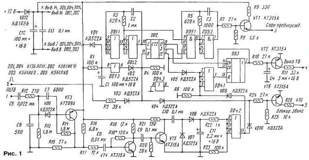
Schematic diagram of the timer is presented in Fig. 1. It contains the node delay (the elements DD1.3, R1. C1, VD1), which does not allow to trigger the timer for transient processes in the TV after turning it on, and sets in the initial state of the counter DD2. performing the functions of the main meter time. In addition, it includes a master oscillator (DD 1.1, DDI.2. R3. S2), the generator 34 (DD5.1. DD5.2, R5, C3) and pulse count pause DD3.
(click to enlarge)
Cascade transistor VT3 allocates and pre-forms from PCTV the sync pulses having a constant amplitude and frequency. Stages transistors VT4 and VT5 reinforce them, diodes VD7, VD8 straighten, and the capacitor C11 constant component stands out. Element DD4.2 plays the role of threshold element.
At the moment the TV is switched on, the capacitor C1 is relatively large capacity discharged and at the exit of the element DD1.3, there is level 1 prohibiting employment counter DD2. All the outputs are 0. The generator 34 to the elements DD5.1 and DD5.2 also does not work. Transistor VT1 is closed. Level 1 at the output element DD4.1 sets the DD3 counter to 0. The key VT2 is closed.
From PCT passing through the coupling capacitor C5, integrating (R12C6R13) and pomerape overwhelming (R14C7VD6) chain emit pulses that amplified by the transistor VT3. Then its collector load (R15, R16) impulses through the circuit R17C8 pass on the emitter-follower transistor VT4. Then through the capacitor C9 they come to the base of transistor VT5, working in key mode.
Diodes VD7, VD8 with capacitor C11 form a rectifier clock. When the absence of the capacitor C11 will be a very small voltage due to interference.
A comparator that distinguish the useful signal, serves as the inverter DD4.2, triggered when the voltage on the inputs above Un",/2. Resistors R22 and R23 form a bit the circuit of the capacitor C11 and a divider that defines the operation of the inverter DD4.2.
When receiving PCTV output element DD4.2 level 0 appears, which is applied via the diode VD9 to the input element DD4.1, is inverted and prohibits the counter DD3. After charging of the capacitor C1 DD2 counter counts down set time interval. On reaching it will start the DD3 counter. defines the time delay switch-off, and the generator on the elements DD5.1. DD5.2. R5, C3, warning sound or light signal when the time is over.
Switching to any other channel after charging of the capacitor C1 will return the device to its original state. Loss of sync causes switching of the comparator DD4.2 to state 1. turns off the speaker system and enables the DD3 counter (without a light or sound alert). After the preset interval of time the TV will turn off. Warning user and switch the TV to happen regardless of the signal, coming from a radio channel, or an external video signal.
The establishment timer basically boils down to the choice of the desired time interval of reference, i.e. one of the outputs of the counter DD2. and pauses (i.e. one of the outputs counter DD3). Due to the fact that the counter DD2 increases the repetition period pulse is stepped twice, intermediate values can be obtained adjusting the frequency of the master oscillator (component values C2 and R3). When the option specified core count lasts about 1 hour 20 minutes, the pause time is 30 C. Moreover, it is not necessary to achieve high accuracy. The main reference comes from the last switching apps.
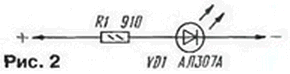
When testing the operation of the device to observe convenient to use chains collected by the circuit of Fig. 2. The first of them, respecting the polarity between include point 3 and the common wire (it is also useful to connect in parallel and any speaker impedance of 4 to 20 Ohms). The second is connected to the collector transistor VT2 and the positive conductor of the power source. The third chain include between point 5 and the positive conductor of the power source.
At power-up timer the third led glows lock sound (open the transistor VT6). and after 15 turns on the second led mode off (opens the transistor VT2). When served PCTV. both LEDs are extinguished. For the acceleration of this process, the capacitance of the capacitor C2 temporarily reduce three times.
To simulate user commands the output of the anode of the diode VD3 short connected to the positive conductor of the power source. In this case, first illuminates the first led and sound an audible signal (activated transistor VT1). after 30 seconds, lights up the second led (off mode when the opening of the transistor VT2). When you change the time and another the DD3 counter output input CP (pin 13) must also be connected to this output. Level 1 it stops the countdown.
In the case of fuzzy actuation element DD4.2 to apply a voltage voltage boost to the anode of the diode VD7, disabling him from the common wire, and is connected to the engine tuning resistor of 47 to 100 ohms. The other two output resistor connected to a power source. By adjusting the resistor to provide clear activation element DD4.2.
The device is designed for connection to TVs and subsequent USCT modifications that contain blocks of colour MC, MC, MC, etc., equipped with remote control system on a chip CRHL, relay ATC-1 and a button for turn off the TV. If SDU is missing, you should enter this in the TV an extra button to turn it off without fixation (P2K or SDH) network switch to replace the button to turn the machine on, and the node turn off the timer signal to be collected by the circuit of Fig. 3 (numbering of elements corresponds to Fig. 1). Setting a node to the TV, be sure to remove the plug and verify correct connections.
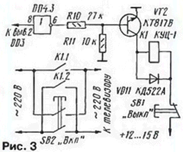
In the TV on a timer set voltage +12 V. Point 1 timer connected to the pin 7 of connector X1 (A1). the video or PCT, and point 2 connects to pin 1 of the chip CHP or pin 4 of the micro CCP. The connection pins are provided for the purpose of exclusion based on the position of the switch APCG, otherwise you'll need to invert the signal. Point 3 connected to the pin 11 of the chip MDA3505 (CAS) or leave the chain with led, setting it on the front of the TV . In this case, will be observed horizontal stripes. You should verify visually in stock resistor 75 Ohm between pin 11 of the chip and GND. Point 4 is connected to the output 12 of the chip CRHL, and point 5 to pin 2 connector X1 (A1) or to pin 8 of the micro UPCS-2.
In the device, except as indicated in the diagram, you can apply chip CLA, CLE, KLN, KIA, KIA transistors, etc. series CT, with KT315 any letter index, diodes KD521, CD. CD, D18, D9 also with any index, resistors sun or MLT, capacitors K73-17. Km. CD. K50-6, K50-12. In the case of the use of elements of microcircuits CLP (shown in diagram) or CLE diodes VD5, VD9 and resistor R6 can be excluded, and the signals from the counter and DD2 element DD4.2 submit on separate inputs of the element DD4.1.
Author: N. Lutchenko, Moscow