Like other types of detectors, the detectors of the type PI (Pulse Induction), constantly improved. As a result of the application of new circuit solutions are able to achieve even higher sensitivity of these devices.
According to the author, the design of the proposed device is quite complex to repeat beginners radio Amateurs. In addition, certain difficulties may arise when the adjustment of this device. Need to pay special attention to what Assembly errors and incorrect instrument setup may cause building expensive elements.
Schematic diagram
A schematic diagram of the improved pulse the detector can be divided into two parts, namely: on the block the transmitter and receiver unit. Unfortunately, the limited scope of this book allows you to elaborate on all the features of the circuit design, used when creating this device. So next will be considered basic operation of only the most important nodes and cascades.
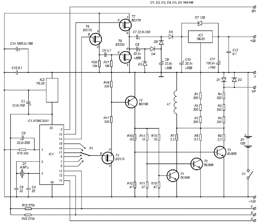
As mentioned, this is an advanced metal detector a variant of the device, discussed in the previous section of this Chapter. Certain modifications to the module of formation of pulses and the synchronization of the transmitter and voltage Converter. Diagram of the receiver unit has undergone more significant changes (Fig. 3.18).
The unit of the transmitter module includes forming pulses and synchronization the transmitter and the voltage Converter.

Fig. 3.18. Schematic diagram of the transmitter unit of the improved pulse metal detector
The main part of the whole structure is a module of generation of pulses and the synchronization is executed on the microprocessor IC1 type ATC ATMEL and ensuring the formation of pulses for the transmitter and signals governing the operation of all other units. Operating frequency of the microcontroller IC1 stable quartz resonator (6MHz). When the specified value of the working the frequency of the microprocessor generates a periodic sequence of governors pulses for different stages of the detector.
Initially the output of IC1/microprocessor 14 generates a control pulse for the transistor T6, after which the output of IC1/15 is formed a similar pulse to transistor T7. Then the process repeats itself again. The result is the launch of a voltage Converter.
Further, consistently on the findings IC1/8, IC1/7, IC1/6, IC1/17, IC1/16 and IC1/18 pulses start transmitter. These pulses have a same length, but each subsequent pulse is delayed relative to previous to a few bars. The beginning of the first pulse generated on the output of IC1/8, coincides with the middle of the second pulse on the output of IC1/15. Using switch P1, you can select the delay time of the trigger pulse transmitter relation to the start pulse.
After a few clock cycles after the end of the pulse at the output of IC1/18 short the gate pulse amplifier-analyzer is formed on the output of IC1/2. In unlike earlier schemes considered in this unit at the same conclusion microcontroller through several cycles formed the second gate pulse.
In addition, the findings IC1/12 and IC1/13 microprocessor generated control the signals for the transistors T31 and T32 now the receiver unit. The middle Manager pulse for the transistor T31 coincides with the middle of the first gate of the pulse at the output of IC1/2, however, the duration of the pulse at the output of IC1/12 almost twice. Wherein said pulse has a negative polarity. Start managing pulse signal at the output of IC1/13 almost coincides with the middle of the second pulse at the output of IC1/microcontroller 14, he ends in a few clock cycles after the end of the second the gate pulse generated at the output of IC1/2. Then on the output of IC1/11 generates a control signal for the transistor T35 acoustic scheme alarm receiver unit. After a short pause, the sequence of control pulses to the respective outputs of the microcontroller is formed again.
Supply voltage +5 V, previously stable chip IC2, is applied to the output of IC1/20 microcontroller.
Voltage Converter, transistors T6-T8 and the stabilizer IC3, provides for the formation of the supply voltage +5 V required for the power receiving part of the cascades. The control signals for the transistors T7 and T8 are formed on the respective pins of the microcontroller IC1, the transistor T8 this signal is supplied via a level Converter, assembled on the transistor T6. Next, the generated supply voltage is stabilized chip IC3, the output of which a voltage of +5 V is supplied to the cascades receiver.
Output stages of the transmitter are made on a powerful transistors T1, T2 and T3. to the total working load, which acts as a coil L1, shunted by a chain of resistors R1-R6. The operation of the output stage transistor controls the transistor T4. Control signal to the base of transistor T4 is supplied with the corresponding output of the processor IC1 through the transistor T5.
As in the previous section on the detector, the momentum generated by the microprocessor IC1 in accordance with laid in his memory the program, through the switch is input to the transistor T5 and then, after the transistor T4, the output stages of the transmitter, transistors T1-T3, and then transmitting coil L1. When in the area coil L1 of a metal object on its surface under the influence of external electromagnetic field, initiated by the transmitted pulse, excited eddy surface currents. The existence of these currents depends on the duration of the pulse emitted by the coil L1.
The surface currents are the source of the secondary pulse signal, which accepted by the coil L1, is amplified and fed to the analysis scheme. Thanks the phenomenon of self-induction the duration of the secondary signal will be greater than the duration of the light radiated by the transmitting coil of the pulse. The secondary form pulse signal depends on the properties of the material from which made the detected metal object. Processing information about the differences of the parameters pulses are emitted and received by the coil L1, provides for the formation of data to the display unit about the presence of a metal object.
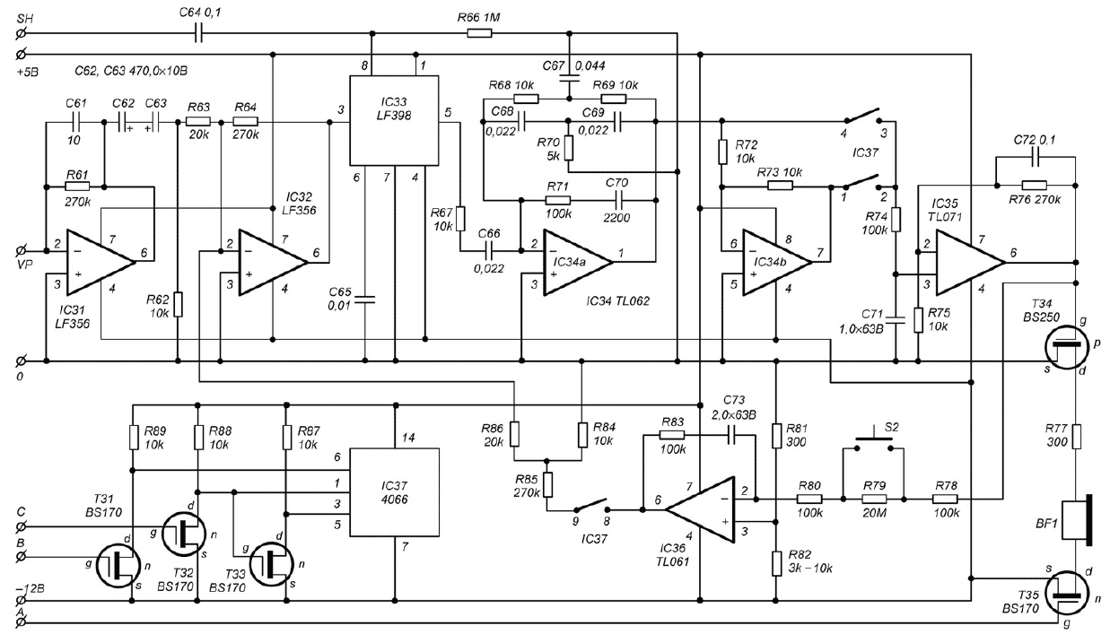
The structure of the receiver unit (Fig. 3.19) includes dual stage amplifier input signal of reference signal amplifiers, amplifier, analyzer, active narrow-band filter, low-frequency diagram of the formation voltage the displacement of the switching circuit and the circuit of sound indication.

Fig. 3.19. Schematic diagram of the receiver unit of the improved pulse metal detector
The signal from a metal object is taken by the coil L1 and through the protection circuit, performed on the diodes D1 and D2 is fed to the input two-stage amplifier with capacitive feedback is made on operational amplifiers IC31 and IC32. With the output circuits IC32 (conclusion IC32/6) amplified pulse signal is fed to amplifier analyzer, made on the chip IC33.
In operation, the instrument amplifier IC33 is always off, and the voltage food is served on him only upon receipt to the appropriate input (pin IC33/8) Gating pulses. At the end of the power output amplifier (pin IC33/5) in a few seconds saved level received signal, recorded during the impact of Gating pulses. Time maintaining the level of the signal depends on the capacity of the capacitor C65. Thus, one input of the amplifier (conclusion IC33/3) is adopted by a pulse signal and a second input (pin IC33/8) through capacitors C64 receives the appropriate gate pulse from module pulse-forming and timing (the output of IC1/2).
Next, the selected signal passes through the active filter is performed on the element IC34a and tuned to a frequency of 6 MHz. To achieve these on principle the circuit parameters of the individual elements of this filter is recommended parallel connection of resistors and capacitors. For example, the value defined in the diagram of capacitance C (0,044 ICF) is parallel the inclusion of two capacitors 0,022 UF each. It should be noted, when using quartz element Q1 with an operating frequency that is different from 6 MHz, the values of the individual elements of the filter should be recalculated.
With the filter output signal is supplied to the synchronous detector, the input of which installed inverting amplifier with a gain of 1, which is made on item IC34b. When using this circuit to the corresponding pairs of contacts chip IC37 (findings IC37/1.2 and IC37/3,4) switch a negative signal applied to an integrator chain with a capacitor S. The control signals for the chip IC37 formed by the cascades, made transistors T31-T33.
From the output of chain integrating the pulse signal passes to the input of the amplifier cascade, which is made on the chip IC35 and simultaneously performs the functions the low pass filter. The voltage drop at the output of the operational amplifier (the output of IC35/6) leads to the discovery of the transistor T34 and the connection to wire headphones BF1. When you receive from the corresponding output the microcontroller (pin IC1/11) on the transistor T35 control signal to phones to listen to the audio signal. Resistor R77 limits the current flowing through the headphones BF1. His selection possible to adjust the volume of the acoustic signal.
The signal from the output of IC35/6 is also fed to the input of another operational amplifier (conclusion IC36/2), whose task is the zeroing of the output signal. It the use is explained by the fact that the output of the chip IC33 changing in time the output signal will be formed, and in the absence in the area the search coil L1 of metal objects, so the amplitude of the resulting the signal will be nonzero. Through resistor R86 to the input of the second the amplification stage (the output IC32/2) is fed offset voltage in the date of receipt of the first Gating pulse. The required level bias voltage depends on the level of the output signal at the output of IC35/6, the formation is provided by an integrating chain S, R78-R80 and the amplification stage IC36 on the chip.
Chain of forming the bias voltage operates only during the circuit corresponding contacts of the chip IC37 (findings IC37/a 9.8). The duration of this time is three clock cycles. Thus the control signals for chip IC37 do with cascades, transistors T31-T33. So ensures the alignment of the levels of signals generated in moments receipt of the first and second Gating pulses. By pressing S2 time the zeroing process can be reduced significantly.
Details and design
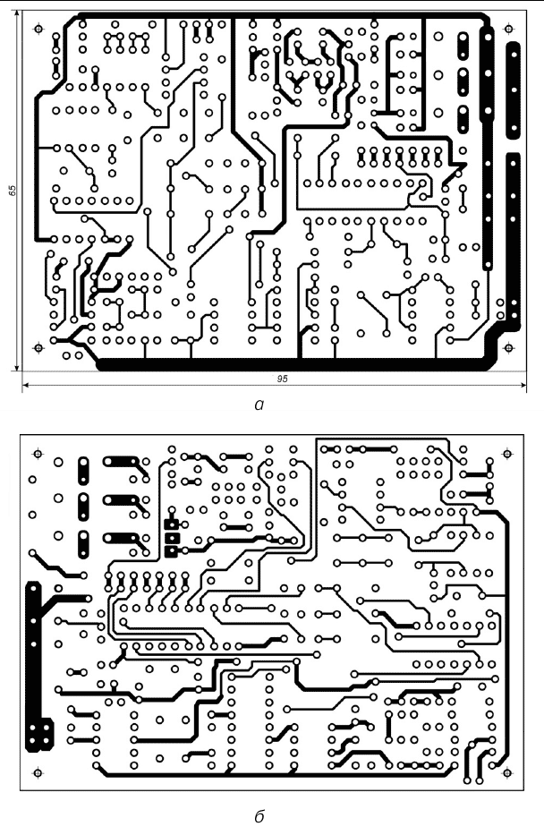
All the details of the proposed instrument (with the exception of the search coil L1, switch R1, switch S1 and buttons S2) are located on a printed circuit Board (Fig. 3.20) dimensions h mm, made of two-sided foil Micarta or PCB.

Fig. 3.20. The printed circuit Board of the improved pulse metal detector
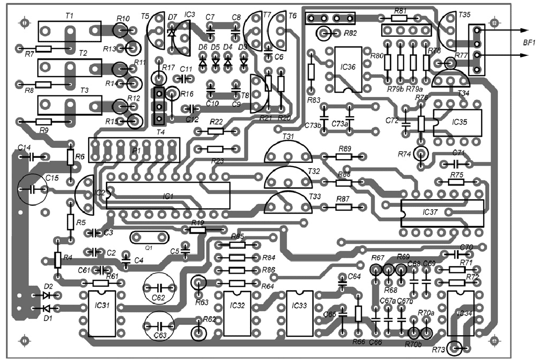
To detail used in this device without facing any special requirements. It is recommended to use any small-sized capacitors and resistors that can be placed on the circuit Board. Need note that to achieve specified in the concept of options individual elements should be used in parallel and resistors capacitors (Fig. 3.21). On the circuit Board for placement of such elements there is also additional space.

Fig. 3.21. The arrangement of the elements of the improved pulse metal detector
Chip type LF356 (IC31, IC32) can be replaced by LM318 or NE5534, but in the result of such a replacement can be problems with establishing. As amplifier IC35, in addition to those listed in the diagram of the chip type IL071 can use of IC CA3140, OR or OR. Chip type R061 (IC36) without problems replaced with the CA3140.
As transistors T1-T3 in addition to specified in the concept you can use type transistors BU2508, BU2515 or ST2408.
The working frequency of the crystal must be 6 MHz. Can to use any other crystal element with a resonance frequency from 2 MHz to 6 MHz. However, in this case you will need to recalculate the filter elements, performed on the element IC34a.
For installation of microprocessor IC1, use a special socket. When this microcontroller is set to charge only once all installation works. This condition must be followed when carrying out adjusting operations related to soldering in the selection of values the individual elements.
Special attention should be given to the manufacture of the coil L1, the inductance of which shall be 500 mcg. The design of this coil is virtually no is different from the structure of the search coil L1, used in the detector discussed in the previous section. It is made in the form rings with a diameter of 250 mm and contains 30 turns of wire having a diameter of not more than 0.5 mm. When you use a larger diameter wire current in the coil will increase, but will grow faster values of the parasitic eddy currents, resulting in deterioration of the sensitivity of the instrument.
It should be recalled that for the manufacture of the coil L1 is not recommended lacquered wire, since the potential difference between adjacent coils when the radiation pulse reaches 20 V. If in the process of winding turns of the coil next will be the conductors, for example the first and fifth windings, insulation breakdown almost assured.
In turn, this may lead to failure of the transistors of the transmitter and other elements. Therefore, the wire used in the manufacture of the coil L1, must be at least in PVC insulation. The finished coil also recommended well to isolate. You can use epoxy resin or various foam fillers.
The coil L1 must be connected to the Board using double-well insulated wire, the diameter of each conductor which shall not be less than the diameter of the wire from which the coil itself is made. Not recommended use coaxial cable because of its greater capacity.
A source of audio signals can be either head phones with resistance from 8 to 32 Ohm small speaker with similar the resistance of the coil.
As the power source B1 is recommended to use rechargeable the battery capacity of about 2 hours, since the current consumed data a metal detector exceeds 200 mA.
Printed circuit Board with the controls it contains and the power source are placed in any appropriate case. On the housing cover mounted switch P1, connectors for headphones BF1 and coil L1 and the switch S1 and S2 button.
Establishing
This appliance should be set up in conditions when any metal objects removed from the search coil L1 at a distance of not less than 1.5 m.
Feature settings and adjustments of the considered detector is that its individual modules and cascades are connected gradually. In this case each operation connection (soldering) is disabled when the source power.
First you want to verify the existence and magnitude of the supply voltage on the corresponding socket contacts of the chip IC1 in the absence of the microcontroller. If this voltage is normal, the next step is to install the microprocessor on the Board and with the help of a frequency counter or oscilloscope to check the signal on the findings of IC1/4 and IC1/5. The frequency of the pilot signal at these pins must match the working the frequency of use of the quartz resonator.
After connecting the transistors of the inverter voltage (no load) current consumption should increase by about 50 mA. The voltage on the capacitor C10 in the absence of load should not exceed 20 V.
Then connect the stages of the transmitter. Modes of operation of the transistors T1-T4 must be the same and are set by selecting the values of resistors R13-R16.
The resistance of the coil L1 is shunted by the resistors R1-R3, should be approximately 500 Ohms. The conclusions of the coils and resistors should be well soldered, since the contact failure in this circuit entails the exit failure of the output transistors of the transmitter.
To test the functionality of the cascades transmitter, you can hold the coil L1 ear and turn the power of the detector. After about half a second (after reset of the microcontroller), you can hear the signal low tone, appearance which is due to the micro-vibration feedback of the individual turns of the coil. When this at the collectors of transistors T1-T3 will be generated unmodulated peaked pulse with a duration of about 10-20 μs, the form of which can check with an oscilloscope. The increase in the resistance of resistors R1-R3 leads to the increase of the amplitude of the output pulse with a decrease in its duration. For the selection of the resistance values of the shunt coil L1 is not it is recommended to use a variable resistor, because even a short the contact failure of the engine with the conductive track may damage the output transistors of the transmitter. Therefore, it is desirable to gradually change the magnitude of the shunt with a step of 50 Ohms. Before replacing parts, be sure to switch off the supply voltage of the device.
Next, you can begin to configure the receiving part. If all parts are serviceable, and the installation is made correctly, after the switching on of the detector (approximately 20 µs after the start of the pulse) at the output circuits IC31 (conclusion IC31/6) with an oscilloscope, you can observe exponentially increasing signal, turning the signal level constant. Distortion of the front of the signal eliminated by choice of resistors R1, R2 and R3, shunt coil L1.
After that, you should monitor the shape and amplitude of the signal at the output chip IC32 (conclusion IC32/6). The maximum amplitude of this signal set the selection value of the resistor R64. In the process of building the bias voltage on the output IC32/2 can be served with a separate divider voltage, which can use a variable resistor 5-50 ohms, included, for example, between pins IC32/a 4.7. A moveable connects to the resistor R86.
The output of the chip IC33 (conclusion IC33/5) one can observe the square wave signal the amplitude of which is temporarily connected potentiometer. Further it is necessary to control the signals at the outputs of elements IC34a and IC34b. When on the findings IC34/6,7 should be the correct sine wave. As a result the capacitor C is formed by a DC voltage is input to chip IC35.
During the configuration process, you can observe the response of the device to change the position engine temporarily connected to the potentiometer, and then instead solder the divider R84, R85.
The order of work
Using a metal detector has no significant differences from the use of a metal detector as discussed in the previous section.
Prior to the practical use of this detector should switch P1 to set the minimum pulse delay. If in the process of work in the area the validity of the search coil L1 will be any metallic object, the head phones will appear acoustic signal. The transition in the mode more pulse delay will ensure the elimination of the influence of not only magnetic properties of soil, but will also eliminate the response of the device to all sorts of extraneous items (rusty nails, foil from cigarette packs, etc.) and subsequent a vain search.
Author: M. V. Adamenko


