


")

The node diagram of which is shown in the figure, can work as a balanced mixer at the reception and as a balanced modulator in the transmission. When receiving the RF signal with a bandpass filter formed by the elements L1, L2, C1-C3, through the coupling coil L3 is fed in opposite phase to the gates of transistors V1, V2, and the voltage of the local oscillator on the sources of the transistors through capacitors C6-C8.
The output node selects the if signal (500 kHz).
When a transmission frequency signal from the transformer T1 in the opposite phase is supplied to the gates of transistors V1 and V2, and the signal of the local oscillator frequency of 500 kHz on their origins. At the output of the mixer thus there is a DSB signal.
Capacitors C4, C5 and inductors L4, L5 divide the high-frequency and low-frequency circuits.
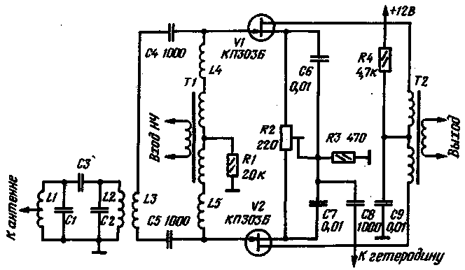
Inductors L4 and L5 are wound resistors MLT-0,5 impedance at least 1 MOhm wire PEL 0.07 (200 turns). The transformer T1 - transition from any pocket receiver, T2 is wound on a ring (outer diameter 7…12 mm) magnetic core of ferrite permeability 400…1000. Each winding comprises at 34-loop wire PEL of 0.09. Winding are three wires, twisted into a bundle.
This mixer can be used in transceiver Radio "-76" instead of the diode ring. In this case, the coil L3 should contain 20 turns of wire PEL 0.14. It is wound on top of the coil L2.
The building site is reduced to its balancing when working on the transfer of the resistor R2. At the same time achieve maximum suppression of the carrier frequency.
Author: L. Kudacki (UB5UKF), POS Klavdiev Kyiv region; Publication: N. Bolshakov, rf.atnn.ru