


")

To reduce the size and weight mains power supplies in recent years more wider use conversion voltage at a frequency of several tens of kilohertz. This source contains a mains rectifier, filter ripple at twice the mains frequency, voltage Converter, step-down transformer, rectifier and filter ripple frequency doubled conversion. The Converter is usually performed according to the scheme of the bridge or half-bridge inverter, in which the transistors are opened and closed alternately via pollperiod switching. The lack of such Converter - the presence of through collector current in the closing moments of the transistors. Because this for them is great instantaneous electric power permissible the value which limits the power of such devices. Valid the instantaneous power is usually used in voltage converters silicon transistors, for example, a series KT, not more than a few hundred watts.
To remove this limitation to some extent allows the use of a bridge inverter loaded series resonant circuit. The transistors of such a device are closed in the absence of collector currents, the maximum voltage at the collector (on respect to the emitter) and the maximum collector current act on the transistor in different times, so the instantaneous electric power generated at him, appears to be small.
The possibility of a bridge inverter series resonance illustrated below the mains unit. It is designed to use as an equivalent of a 27-volt onboard network of the car (when active or inductive-resistive load).
Schematic diagram of the device shown in the figure. Its main units - filter C1L1C2 preventing penetration into the network interference from the frequency Converter; a rectifier network the voltage on the diodes VD1- VD4 with filter C3-C5L2C6 - C8; bridge inverter transistors VT1 - VT4 with a resonant circuit L3C10C11, step-down transformer 74, the rectifier voltage of high frequency diodes VD13-VD18 with filter C12-C15L4C16C17; a control unit inverter circuits DD1-DD4 and transistors VT5, VT6 and two supply source: unstabilized (VD19) and stable (VD20 DA1). HL1 led - indicator switching the unit to the network.
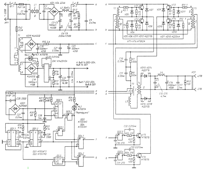

The management host bridge inverter consists of a clock pulse generator, performed on the single vibrators DD1 chip, dispenser pulses on the trigger DD2.2 and the elements of the IC DD4, two amplifiers (DD3.3; VT5 and DD3.4, VT6) and devices to protect the unit from overload (VD21, DD2.1) with synchronizer (DD3.1, DD3.2). The led signals HL2 actuation of the protection device.
When you turn the unit into a network switch Q1 is supplied with voltage on the control node, and the inverted output of single-shot DD1.2 there are positive pulses duration of 17 μs with a constant repetition frequency of about 40 kHz. The trigger DD2.2 logical 1 signals arising at its forward and inverse the outputs alternately opens "elements DD4.1, DD4.2. and the pulses arrive at the the input of one amplifier (DD3.3, VT5), then another (DD3.4, VT6). In the result of the opening pulses polarity served on the emitter junction transistors VT1, VT4, VT2, VT3.
After a while after the appearance of the clock pulses (delay caused quite a large filter time constant C3-C5L2C6-C8) the capacitor C9 occurs smoothly increasing rectified voltage and inverter converts it into an alternating voltage of a frequency of 20 kHz, is applied to the winding I transformer T4. The voltage taken from its winding I, rectified by diodes VD13-VD18 and through the filter C12-C15L4C16C17 is supplied to the load. Resistor R13 reduces the output voltage of the unloaded rectifier.
The performance of the inverter can distinguish four phases. First, duration of 17 MS, open the transistors VT1, VT4, and capacitors C10, C11 is charged through them, the primary winding of the transformer T4 and the inductor L3. The current in this circuit initially increases from zero to maximum values, then, as the charging of the capacitors decreases to zero. The form of the current recalls the half cycle of the sine wave.
In the second phase, lasts 8 MS, to bases of transistors VT1, VT4 is served voltage closing polarity, and they are closed.
In the third phase (as first, duration of 17 MS) open transistors VT2, VT3, and to each of the closed transistors VT1, VT4 is applied almost all rectified by diodes VD1-VD4 voltage (at a load resistance of 1 Ω to about 260 In). Current recharge capacitors C10, C11 to the maximum voltage of the opposite polarity the same as in the first phase, flows through the serial circuit formed by the capacitors, inductor L3 and the primary winding of the transformer T4. The voltage to which they recharge depends on the load resistance: the smaller it is, the more this voltage (at a load resistance of 1 Ohm - about 200).
When the collector current of the transistor VT2, VT3 is reduced to zero, begins the fourth phase of operation of the inverter, lasting, and the second, 8 ISS: bases of the transistors of the windings of transformers T2 and T5 is supplied with a closing the tension. Transistors VT1, VT4 all this time continue to be closed. The pause is necessary in order transistors VT2, VT3 is completely closed and when the lid of the transistors VT1, VT4 not have any momentum through current through the transistors adjacent shoulders. Due to that the switching voltage is supplied to the emitter transitions in the moments when collector current no, instantaneous electric power collector the transition in the worst case no more than a few watts.
Node protect the unit from overload operates as follows. After filing voltage trigger DD2.7 is set in one state (on the inverted output - voltage logic 0), and the output element DD3.2 (conclusion 11) there is a voltage logical 1, creating the conditions for passage the clock pulses through the elements DD4.1 and DD4.2 In this state, the trigger all the time while the power delivered to the load, less than 1 kW.
Upon reaching the ultimate capacity of the amplitude of the first pulse received at the counting input trigger DD2.1 the secondary winding of the transformer T3 through the bridge VD21, is sufficient to convert the trigger to the zero state (at the inverted output - voltage logic 1). Change low logic level high on top the schema of the input element DD3.2 leads to the fact that with the arrival of the next clock pulse at its output voltage is set to logic 0, and the passage pulses through the elements DD4.1, DD4.2 stops. Thanks RS-trigger on the elements DD3.1, DD3.2 prohibition signal appears only at the beginning of the pause between pulses, which prevents the output transistors of the inverter out of operation (closing in the presence of the collector current would lead to failure due to excessive increase of the instantaneous electric power). The site protects the transistors of the inverter and short circuit load.
To return the PSU to its original state after tripping him need to disable and re-enable the switch Q1. When turn off the unit filter capacitors C3 - C8 is discharged through resistors R1 and R2. It necessary to ensure that during the rise time of the pulse amplitude of the base current transistors VT1 - After VT4 re-enable when they are not fully open (i.e. not included in the mode saturation), their collectors was not immediately a large voltage capable lead to failure.
In the resonant circuit of the inverter capacitors applied (C10, C11) K71-4 for a rated voltage of 250 V. the filter Capacitors C12-C15 - K73-16 rated voltage 63 V. the Resistor R13 - sew-10. The rest resistors and capacitors may be of any type. The switch Q1 - TB1-2.
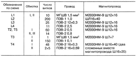
In the power source control unit applied uniform transformer TN 127/220-50. All other transformers and chokes the device is hand made. Winding data given in the table. The inductor L3 and both windings of the transformer T4 is wound twisted wires into a bundle. To reduce leakage inductance of the transformer winding II is wound two held together by bundles. The allotment received by the output connection of the beginning of one of Polubotok with the output end of the other.
The cores of all chokes are assembled with non-magnetic gap of 0.5 mm.
The control node of the inverter and its power source are mounted on a printed circuit Board from a foiled fiberglass thickness of 2 mm. most of the remaining parts block mounted in hinged manner on three boards dimensions mm 220x85 from PCB thickness 3 mm: on one of them pinned diodes VD1- VD4 and the components of the filter C1L1C2 and C3-C5L2C6-C9, other transformers T2, T3, T5 and the details of the inverter, the third inductor L3 and filter details C12-C15L4C16C17.
Transistors VT1 - VT4 installed on the dural heat sinks in the form of plates dimensions mm 70x60x8 (parties Hm they are attached to the circuit Board), diodes VD1-VD4 - on U-shaped heat sinks bent from aluminum plates dimensions 100x25x1,5 mm, diodes VD13…and VD18 transformer T4 - ribbed dural the heatsink area a cooling surface of about 1000 cm2, mounted in the rear of the case block.
Establishing device start without fuse FU1. Turn the power node control the oscilloscope is satisfied on the emitter transitions transistors VT1-VT4 pulses of positive polarity duration of 17 μs with the repetition frequency of about 20 kHz (oscillation period of approximately 50 μs). When connecting any output secondary winding of the transformer 73 positive to the positive output of the power source circuits node control these impulses should disappear.
Then disable the output of the inductor L3 from the primary winding of the transformer T4. establish into place the fuse FU1, and instead of the contacts 7 and 8 network switch Q1 include milliammeter. The current consumed by the inverter without the load should be no more than 15 mA. After this, connect the findings the inductor L3 and the primary winding of the transformer T4 additional resistor resistance of about 0.5 Ohms, otpaivaete network conclusions rectifier bridge VD1 - VD4 from the inductor L1 and fed to them from the adjustable autotransformer (for example, Latri) variable voltage 20…30 V. the output of the unit connect the dummy load resistor a resistance of 1 Ohm with power dissipation 700…800 watts. Controlling oscilloscope the waveform on the additional resistor, choose non-magnetic gap in the magnetic circuit of the inductor L3, the pulses (both positive and negative polarity) on the screen to become more like half of a sine wave.
Further, watching pulse shape, increase the voltage at the input of the bridge VD1 - VD4 to 220 V. the output power to the dummy load increases up to 650 700… W, however, the pulse shape should remain practically unchanged. If such power they sharpened, it indicates the saturation of the magnetic circuit of the inductor L3 or transformer T4 and must be replaced more massive (big cross section).
Finally, deletion of the circuit further resistor, choose a resistor R18 such a way that the node overload protection is triggered when the output power of 1 kW (it is obtained by reducing the resistance of the dummy load).
While establishing should observe the safety rules, as many circuit block power, in particular, under control of the oscilloscope, there are high voltage.
Load capacity of up to 700 watts can be connected directly with the output of the unit and switch the power the toggle switch. If a higher capacity, it is desirable to provide additional the switch in the load circuit and to connect the first unit to the network, and then load to his exit
Author: S. Tsvetayev