


")

In the present article describes a powerful pulsed source to power various electronic devices. It is built on a half-bridge inverter-driven CHI-controller TL494.
The emergence of powerful high-voltage field-effect transistors was a prerequisite for the development of a network of high-frequency power supplies with latitudes-but-pulse (CHI) control [1,2]. The main advantages of such sources over traditional linear - getting more power at the load with a smaller size and, accordingly, greater efficiency [3].
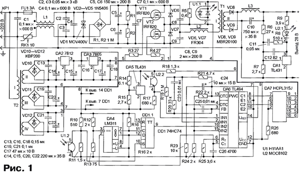
Diagram of the switching power supply unit shown in Fig. 1. The basis device - Converter, assembled on a half-bridge circuit. In the source power is made complete galvanic isolation between the input voltage and output circuits. The control unit is assembled on the basis of CHI-controller TL494.
(click to enlarge)
Main technical characteristics of the power source
- Output voltage, V......28
- The maximum load current, And......10
- Nominal conversion frequency, kHz......100
Transistor optocoupler U2 provides galvanic isolation in the circuit negative feedback voltage. The voltage drop across the resistor R7 approximately 2.5 V. the Resistance of this resistor is calculated, given the current through the resistive divider R6R7. The resistance of the resistor R6 calculated by the formula
where Uвыx - output voltage of the power source; I1 is the current through the resistive the divider R6R7.
The resistance of the resistor R9 determines the current through the emitting diode of the optocoupler U2.1, and minimum operating current stabilizer DA1. When selected the current in this circuit I2 (current value must be within acceptable limits for stabilizer DA1) the resistance of the resistor R9 is calculated by the formula
where F U is the voltage drop on-emitting diode of the optocoupler U2.1.
Chip DA5 stabilizes voltage 8 V to power divider, consisting of phototransistor optocoupler U2.2 and resistor R17. The voltage from the midpoint of the the divider is fed to the noninverting input of the first error signal amplifier CHI-controller DA6.
The voltage to power the control unit and driver (chip DA7) field transistors provides an auxiliary power source on a network transformer T2 and the analog voltage DA2 and DA3.
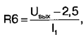
Node protection current collected on the comparator DA4 and the trigger DD1.1. Sensor function current performs the resistor R5, is included in the diagonal of the half-bridge. On the non-inverting the input of the comparator DA4 voltage is triangular in shape with a capacitor (C26) castorocauda chain SHI clock generator-controller (Fig. 2). The output comparator generated clock pulses received at the input of the trigger DD1.1.
If the voltage drop across the resistor R5 will reach 1.1 V, emitting included the diode and the phototransistor of the optocoupler U1. The input S of the flip-flop DD1.1 will go the low level. The true output of flip-flop DD1.1 and, therefore, the noninverting input of the second error signal amplifier CHI-controller DA6 established a high level. In this case, both transistors VT1 and VT2 are closed.
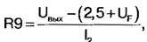
For control of power switching MOSFET applied a specialized chip - dual-channel driver DA7. In Fig. 3 shows the internal structure of one channel. In parentheses are the numbers of the conclusions of the second of the channel. Each channel contains an optocoupler and a powerful amplifier with current output. Such circuits are widely used to manage asynchronous the DC motors.
Driver settings allow you to directly control field-effect transistors with insulated gate switching current up to 50 a at a voltage of not more than 1200 V.
The main parameters of the chip HCPL315J
- Maximum peak output current, And......0,6
- Maximum output voltage, ......1
- Maximum consumption current, mA......5
- The interval of the supply voltage, .......15…30
- Working temperature range, °C......-40…+100
The resistance of resistors R3 and R4 in the gate circuits of the switching transistors calculated according to the formula
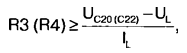
where UC2o (C22) - supply voltage of the driver (the voltage on the capacitor C20 or C22); UL - output voltage driver; lL - maximum peak output current.
In the diagonal of the half-bridge is enabled on the primary winding of the transformer T1 and the inductor L2 (the inductance of the inductor may include a leakage inductance transformer) [4]. The transformer is formed on the yoke e-E size F-43515 of Magnetics Inc. The primary winding 38 of turns of wire #19AWG, and the secondary - 5+5 turns, wound wire #12AWG. The Inductor L2 is wound on the yoke F-41808EC of Magnetics Inc. The winding of the inductor L2 consists of 8 turns of wire #19AWG.
The inductor L3 is made on the magnetic core in a toroidal shape MRD A company Magnetics Inc. The winding of the inductor L3 has 20 turns of wire #12AWG. The throttle input filter L1 - A company Coilcraft, its inductance - 900 mH.
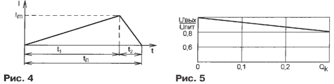
When you turn on the transistor VT1 (or VT2) through the primary winding of the transformer T1 during a control pulse t1 begins to flow linearly increasing current (Fig. 4). When the transistor VT1 (or VT2) is closed, due to the accumulated in the primary winding of the transformer and the inductor L2 of energy in the circuit at time t2 in this same direction continues to flow linearly decreasing current. He closes through the diode VD7, if turned off, the transistor VT1 (or through the diode VD6, if turns off the transistor VT2).
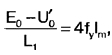
Not taking into account the active power losses in the circuit of the primary winding of the transformer, write equations for the time intervals t1 and t2:
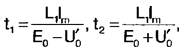
where E0 = u n and m/2 is half of the supply voltage; U'0 - output voltage source provided to the primary winding of the transformer; L1-total the inductance of the primary winding of the transformer T1 and inductor L2.
Hence, we obtain expressions for time t1 and t2 (see Fig. 4):
where lm is the maximum current in the primary winding of the transformer.
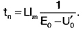
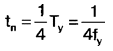
The current flow through the primary winding of the transformer in one direction tn = t1 +t2 can be expressed as follows:
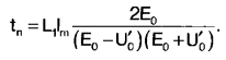
If we accept that
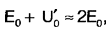
the current flow is equal to
From this equality we obtain the equation for the external characteristics of the source power. For example, the duty cycle of the control pulses
should
where
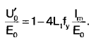
If we denote

then the equation of the external characteristics of the power source has the form

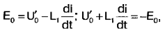
External characteristics of the power supply unit shown in Fig. 5. The output voltage the source depends on the resistance of the resistor R17 is less than the resistance, the less than the output voltage. Current protection operation is determined by the resistance sensor - resistor R5.
Literature
Authors: R. Karow, S. Ivanov, Sofia, Bulgaria