


")

the laboratory power supply of radio equipment is the result of practical the activities of a small group of guys from teenage radio club "Radar" (Penza). It is of interest to those involved in the development of instrumentation op amps and the modern chips that require one and bipolar supply voltage, regulated within a rather broad range.
A feature of this laboratory power source is node protection. It is known that for some circuits that are powered from the source bipolar voltage, it is not acceptable that one of them is absent. To avoid such situations in the proposed unit provides protection system, the locking operation of any one of the shoulders of the feeding device when the closure is in the other your shoulder. After removing the cause of the circuit power source automatically goes into normal operation.
Technical characteristics of the device
- The limits of regulation of the output voltage, ......+1,25…18
- The throttle limits the load current, And......0,01 1,2…
- The level of fluctuations in the source mode current at IR=0.1 A, mV......10
- The voltage threshold lockout devices, ......1
The instrument parameters of the voltage source correspond to the reference data used in the integrated circuit voltage regulators [1, 2].
Structurally, it consists of two functionally complete units: bipolar power loads and node protection circuit mounted on separate circuit boards.
The scheme of the first of these blocks is shown in Fig. 1. Winding II and III network transformer T1, diode bridges VD1 - VD4 and VD5 - VD8 form a source bipolar unregulated voltage +23…24 V, all nodes of the supply and the blocks of the device. Power source circuits DA1 at its negative terminal of the serves as a voltage regulator R11VD14 and chips DA3 - stabilizer R1VD9.
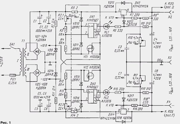
The operation and circuitry of both shoulders of the symmetric power source, therefore, a more detailed look at the work of only one of them is positive.
Nestabilizirovannoy unipolar voltage (maximum +25), pulsations which smooth out the capacitors C1 and C2, through the measuring resistor R5, which is measuring bridge formed by the resistors R2.1 - R5 and the Zener VD10 and VD11, is applied to the input (pin 2) integrated stabilizer DA2 output voltage adjustable variable resistor R10. Power measuring the bridge provides a current source implemented on a field-effect transistor VT1.
While the output current of the stabilizer is less than the set value, the fall the voltage across the resistor R5 is small, the voltage on the direct output DA1 more than inverted, and the output 6 of the shelter voltage close to +21 V. the Diodes HL1 and VD13 closed and have no effect on the operation of the stabilizer DA2.
If the output current becomes equal to the threshold value set resistor R2.1, the work included measuring bridge. Oh DA1 enters linear mode in which the equation
UR2.1 + UR3 = UR5 + East VD10.
In this case, the output voltage of the shoulder will depend on the voltage at the output The shelter, which in turn monitors the voltage drop across the resistor R5, ie the load current when running the above equality. Therefore, when the ratio R3/R4 = 1 and East VD10 = East VD11
IR = R2.1/R4.East VD11/R5.
This simplified formula can be used if the need arises to recalculate the parameters of the measuring bridge in the light of available element base or other requirements. For more accurate tracking of smaller load currents the resistance of the resistor R5 is desirable to increase. While correspondingly decrease the upper limit of the load current.
Fundamentally it works shoulder and negative power source.
The block diagram of the protection device against short-circuit at the output or load is shown in Fig. 2. When applied to the input of the bipolar output voltage transistors VT4 and VT7 open and thereby shunt: transistor VT4 - chain, formed by HL3 led, resistor R25 and radiant diode of the optocoupler U1 and transistor VT7 - chain HL4, R29 and the led of the optocoupler U2. Transistors VT3 and VT6 in this time closed. The elements of these circuits protection system corresponds to the device without fault in his external circuits.
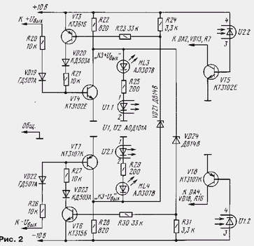
Assume that the circuit has occurred in the load connected to the output of the positive leverage the power source. In this case, the transistor VT4 is closed. This leads the opening of the transistor VT6 (through the Zener diode VD24 and resistor R30) that eliminates the mutual locking of the protection system. Transistor VT7 after blocking minus the shoulder remains open current supplied to its base through a resistor R27 and diode VD23. At the same time open HL3 led signaling the emergence circuit +Uвых, and the emitter of the optocoupler U1. As a result dramatically increases the current of the photodiode of the optocoupler, the transistor VT8 and current manifold blocks the stabilizer DA4 minus the shoulder of the device.
It works and is similar to block part of the protection circuit on the load minus the shoulder of the device. The same threshold triggering unit of the voltage protection is determined by the total voltage drop across the diode VD19 (VD22), emitter the junction of transistor VT4 (VT7), the resistor R20 (R26) and in our case is approximately 1 V. to Increase the voltage by replacing the diodes respective Zener diodes and the selection of resistors R20 and R26 on reliable the opening of transistors VT4, VT7.
Since the output voltage is blocked stabilizers DA2 and DA4 not exceeds 1.3, the resistors R21, R23, R24, diode VD20, a Zener diode and VD21 the transistor VT3 plus shoulder, and similar items minus the shoulder you can exclude as interlocking shoulders will not happen. Provided these same elements for the case when it is necessary to increase (minus shoulder - decrease) the voltage threshold. Thus it is desirable to detach from him and the supply voltage %10 V. it is impossible Otherwise to set the output voltage less than the threshold value, since the protection unit will record the circuit on the load and block the opposite shoulder. The PSU will work without a system of protection.
Its circuit Board is made of one-sided foil fiberglass. The placement of the parts shown in Fig. 3. All fixed resistors - MLT, variables R2.1 and R2.2 - dual resistor CP3-4m group A, R10 and R17 is the same group A, but single. Oxide capacitors C1, C2 and C5, C6 - C50-35, C4, and C8 - K53 series, C3 and C7 - any ceramic, for example km-6. Diodes KDA (VD1-VD8) interchangeable on a similar series CD and CDA (VD12, VD18) - any of a series CD, CD, CD, diodes and VD13 VD17 - any low-power silicon. Nominal voltage stabilizing Zener VD10, VD11 and VD15, VD16 (DE or series X) can be selected in the range of 9…11 In with a minimal heat the drift.
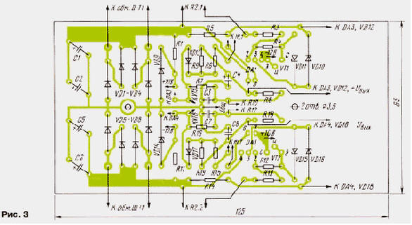
Field-effect transistors VT1 and VT2 (KP with letter A, b, or W) it is desirable to select the initial current flow is in the range of 2…4 mA.
Mains transformer T1 is used in the device of the disassembled unit power of foreign production. Will fit any other, including homemade providing on each of its secondary winding AC voltage 17…18 In load current of at least 1.4 A.
Zener VD11 and VD15 are from the printed conductors of the Board. Stabilizers DA2 and DA4 mounted on a finned heat sinks, which screws mounted on the circuit Board from the other parts. For best thermal contact stabilizers previously covered with a layer of heat conducting paste.
The establishment of the main unit of the device is disabled when the block protection and is careful check of the installation and all connections and, if necessary, to fit voltage providing circuits, and configuration of the measuring bridge.
Immediately after you connect the device to the network should first be measured voltage filtering capacitors C1, C2 and C5, C6, smoothing ripple the bipolar rectifier and the Zener VD9, VD14, providing food shelter DA1 and DA3. The voltage on the capacitors must not exceed +25 V, and the Zener is to be within +9,5 10,5…V. During rotation of the shafts of resistors R10 and R17 voltage at corresponding outputs of the shoulders of the PSU should smoothly to change from 1.25 to 18 In, and the LEDs HL1 and HL2 not to burn. The maximum values of these voltages set by the selection of resistors R8 and R18.
The function of the measuring bridges shoulders devices control high resistance DC voltmeter, connected to the input terminals of the shelter DA1 and DA3. The voltage at the inverted input of each of the OS (relatively common wire) should to be a negative voltage at the noninverting input. The difference in the levels of these voltage will change in proportion to the resistances of the resistors R2.1 and R2.2 "Limitation IOUT". At equal voltages, the device must to switch from the voltage source mode current source (or Vice versa).
The initial value constraints of the load current (0.01 A) making the selection respective resistors (R3 and R13) measuring bridges in the position of the shaft variable resistor R2 in the position of minimum resistance.
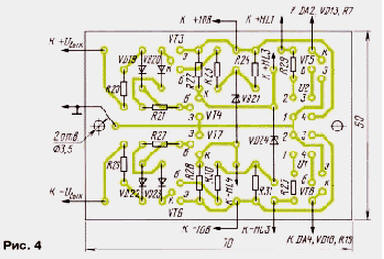
The printed circuit Board of the protection unit, the placement of parts on it and connect to the Board power supply depicted in Fig. 4. All resistors - MLT-0,25. The transistor VT3 - any of a series of K, and VT6 - any of a series of KT315. The current transfer ratio the base of transistors CTE (VT4, VT5) and CTC (VT7, VT8) should not be less than 400.
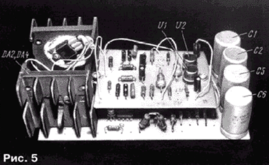
Circuit Board power supply unit, fastened like a stack (Fig. 5), and mains transformer placed in the enclosure with internal dimensions mm 210x90x90 from textolite plates with a thickness of 5 mm.
All the elements and controls of the unit, and also socket-terminals for connecting the load and grounding submitted for facial panel (Fig. 6).
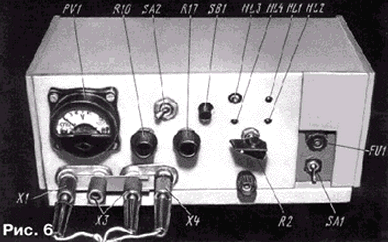
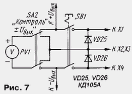
There is also a DC voltmeter (PV1 on Fig. 7), allowing you to control the output voltage of any of the arms of the block power.
The power dissipated by the circuits DA2 and DA4, shall not exceed 10 watts. This limits the maximum output current of the current source value 1.2 A at the output voltage of more than +15 V. At lower output voltage drop the voltage on these chips is increased, the allowable output current decreases and when the output voltage of 1.25 V is 10/(24-1,25)=0,44 A. Each pair of Zener VD10, VD11 and VD15, VD16 can be replaced by one Zener voltage 10…15 V. the Half voltage of the Zener diode for supplying the non-inverting inputs of the shelter DA1 and DA3 should be obtained using the divider of the two identical resistors 68 ohms, inclusive, as the Zener diodes in the diagram Fig. 1. The use of thermostable Zener't justified, since they are only at an operating current of 10 mA, and here the current through them is much less.
When the unit is in constant voltage mode when the output voltage of 1.25 V the closing bias on the LEDs HL1 and HL2 is about 20 In that for them unacceptable. Therefore, consistently with each of them should include any low-power silicon diode or just don't install the resistors R9 and R19. Zener VD21 and VD24 for secure closure transistors VT3 and VT6 needs to have a guaranteed higher voltage stabilization than VD9 and VD14, so it is better to use them with the indices of G or D. in order For the transistors VT5 and VT8 not open reverse dark currents of the photodiodes U1.2 and U2.2, the transitions base-emitter should shall be shorted resistors 510 to 680 ohms.
Literature
Author: A. Musakov, Penza