


")

Under the headline "Radio", 1998, No. 5 published a description of a simple power supply circuits series KR. A feature of the new version of the block is capable of smoothly the tolerance limit of the output current from a few milliamperes to a maximum value.
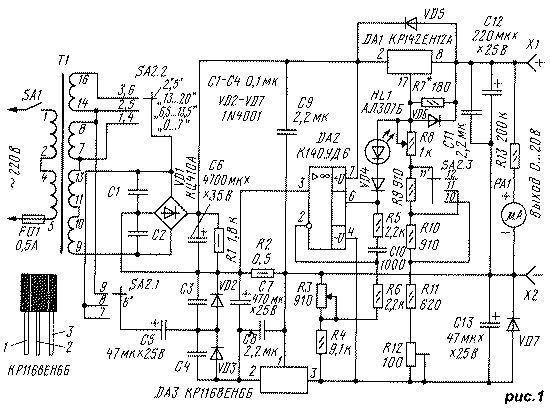
The main difference between the modified power supply (Fig.1) is the introduction of the operational amplifier DA2 and installation chip regulator negative voltage -6 V is -1.25 Until V. the output current is small and the voltage drop across current sense resistor R2 less than the fixed resistor R3, the output 6 of the shelter and on the input circuit DA1 (pin 2) voltage values are approximately equal, the diode VD4 closed and SCS participates in the operation of the device. If the voltage drop across the resistor R2 will be larger than the resistor R3, the voltage at circuit output DA2 reduced, opens diode VD4 and the output voltage of the unit is reduced to the value corresponding to the set current limit. The transition block in the constant current mode is indicated by led on HL1.
As in the mode of short-circuit output voltage OU should be less than -1.25 In about 2.4 In (drop voltage across the diode VD4 and led HL1), the voltage of the negative power source OS is selected equal to -6 V. This value is necessary for all positions of the switch SA2, so I had to switch and input rectifier VD2, VD3.
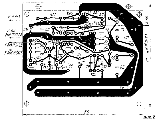
Chip CREB can be replaced by similar with index And, on MC79L06 index BP, CP and ACP, and CREA(B) (see article: A. Nefedov, Walewski A. "Integrated circuit stabilizers series CR" in "Radio", 1995, No. 4), KREN, AN7906, µA7906, but they have the size and the distance between pins more (like CREE). The Pinout is the same. Chip interchangeable on COD CRUD, COD, CRUD. The led may be any type of red the glow. Resistor R2 to four parallel-connected C2-29B 2 Ohm, 0.125 W. To the accuracy of its resistance no requirements, so the resistor can be made independently and cut from high resistance wire. Resistor R12 - CP3-19a. The remaining elements are the same as in the basic version of the unit, similarly, and engineering design. Drawing of the PCB is shown in Fig.2.
The resistors R3 and R4 may be different from those indicated in the diagram twice, it's only important that their relationship was 1:10. The resistor R3 can also be replaced by two series-connected, wherein the second resistance should be 5…10% of the first, it facilitate accurate adjustment of the current limit.
When you configure the unit by the selection of resistor R7 set the output voltage of 20 V and adjust R12 is 0 V. Since these operations are interdependent, they must be repeated several times.
In the mode of the current stabilizer switch SA2 should be installed in the position corresponding to the minimum voltage, which provides the necessary load current. The block will to stabilize the current and at higher voltage, but the power allocated to chip DA1, exceeds the maximum allowable (10…12 W), and may to trigger the thermal protection built into the chip DA1.
Publication: N. Bolshakov, rf.atnn.ru