


")

To adjust or repair of electronic devices you need to have a few power sources. Many homes already have such devices, but, as a rule, they have limited operational capabilities (permissible load current up to 1 A, and if provided for overcurrent protection, she or without inertial adjustable - trigger). In General these sources in their technical characteristics cannot compete with industrial units power. Buy a universal laboratory industrial source quite expensive.
The use of modern circuitry and elements allowed to do in home the power source on the main technical characteristics are not inferior to the best industrial designs. It can be easy to the manufacture and configure.
The basic requirements to be satisfied by such a power source: voltage adjustment in the range of 0 To 30; the ability to provide the current in load up to 3 And with minimum pulsations; adjustable response current protection. In addition, the fault current must be sufficiently fast, to prevent damage to the source in case of a short circuit on output. A stepless adjustment of the power source current limit allows when you configure external devices to prevent any damage.
All these requirements satisfies the following proposed scheme universal the power source. In addition, this power unit can be used in as a stable source current (3 A).
Main technical characteristics power supply:
- stepless adjustment voltage in the range from 0 to 30;
- voltage ripple at a current of 3 And not more than 1 mV;
- adjustable current limiting (protection) 0 to 3 A;
- the coefficient of voltage instability is not worse than 0,001%/V;
- the coefficient the current instability better than 0.01%/V;
- The efficiency of the source is not worse than about 0.6.
The electrical circuit of the power source, Fig. 4.10, consists of control circuits (unit A1), transformer (T1), the rectifier (VD5…VD8), power regulating transistor VT3 and the switching unit of the transformer windings (A2).
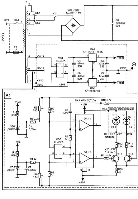
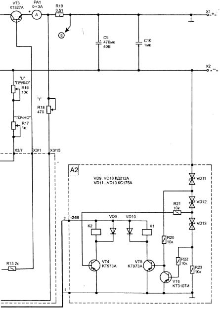
Fig. 4.10. The electrical circuit universal power supply
The control circuit (A1) consists of two General-purpose operational amplifiers (OC) located within the housing, and is powered by a separate winding of the transformer. This allows adjustment of the output voltage from zero, and also more stable operation of the entire device. And to facilitate heat the mode of operation of the power regulating transistor applied with transformer partitioned secondary winding. Bends automatically switch to depending on the level of the output voltage by means of a relay K1, K2, allows, despite the large load current, to apply a heat sink to VT3 small size and to increase the efficiency of the stabilizer.
The switching unit (A2), with only two relays to actuate a switch the four taps of the transformer performs their inclusion in the next sequence: exceeding the output voltage level of 7.5 - included K1; in excess of $ 15 is included In K2; in excess of 22 In - disconnects K1 (in this case, the windings of the transformer receives the maximum voltage). These thresholds are set used by Zener (VD11 .VD13). Disabling the relay when the voltage is in reverse sequence, but with a hysteresis of about 0.3 V, i.e. when the voltage will be reduced by this value lower than when switched on, which eliminates the bounce when switching of windings.
The control circuit (A1) consists of a voltage regulator and a current regulator. If necessary, the device can operate in either mode. Mode depending on the position of slider G (R18).
A voltage regulator is assembled on the elements DA1.1-VT2-VT3. The circuit works stabilizer as follows. The desired output voltage is set resistors "roughly" (R16) and "precise" (R17). In the voltage signal feedback voltage (-Uoc) from the output (x2) through a divider resistors R16-R17-R7 is supplied to the noninverting input of the operational amplifier DA1/2. For the same input through resistors R3-R5-R7 is supplied reference voltage +9 V. At the moment of switching circuits at the output DA1/12 will increase positive voltage (through the transistor VT2 comes to managing VT3) as long until the voltage on the output terminals X1-x2 reaches a set resistors R16-R17. Due to the negative feedback voltage, coming from the output x2 of the input of the amplifier DA1/2, perform stabilization the output voltage of the power source.
The output voltage is determined by the ratio:

where  .
.
Accordingly, by changing the resistance of the resistor R16 ("rough") and R17 ("exactly"), it is possible to change the output voltage IOUT from 0 to 30 V.
When the output of the power supply connected load, in its output circuit current begins to flow, creating a positive voltage drop across the resistor R19 (relative to the common wire of the scheme). This voltage is supplied through resistor R18 at a connection point R6-R8. With the Zener diode VD2 through R4-R6 is supplied reference a negative voltage (-9 C). Operational amplifier DA1.2 amplifies the difference between them. While the difference is negative (i.e. the output current is less than a set resistor R18 value), the output DA1/acts 10 +15 V. the Transistor VT1 will be closed and this part of the scheme has no effect on the operation of the stabilizer voltage.
When you increase the load current to a value at which the input DA1/7 appears a positive voltage, the output DA1/10 will be a negative voltage and transistor VT1 slightly open. In the circuit R13-R12-HL1 current flows, which reduce opening the voltage at the base of the regulating power transistor VT3.
The illumination of the red led(NO) signals the transition diagram in mode current limitation. In this case, the output voltage of the power source drops to a value at which the output current will have a value sufficient for voltage feedback current (IOP), remove the resistor R16, and support at the point of connection of R6-R8, R18 mutually compensate ie appeared zero potential. As a result the output current of the source will be limited at the level set by the position of the slider of the resistor R18. The current in the output circuit is determined by the ratio:
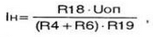
where  .
.
Diodes (VD3) at the inputs of operational amplifiers provide protection chip from damage in case of inclusion without feedback or damage the power transistor. In operation, the voltage at the inputs of the shelter close to zero, and the diodes have no effect on the operation of the device. Capacitor C3 limits the amplified frequency band OS that prevents the excitation and increases the stability of the scheme.
Design features
Parts of the diagram, the dotted (nodes A1 and A2), are located on two printed boards size 80x65 mm from unilateral fiberglass thickness of 1…3 mm.
For node A1 topology and arrangement of elements shown in Fig. 4.11.
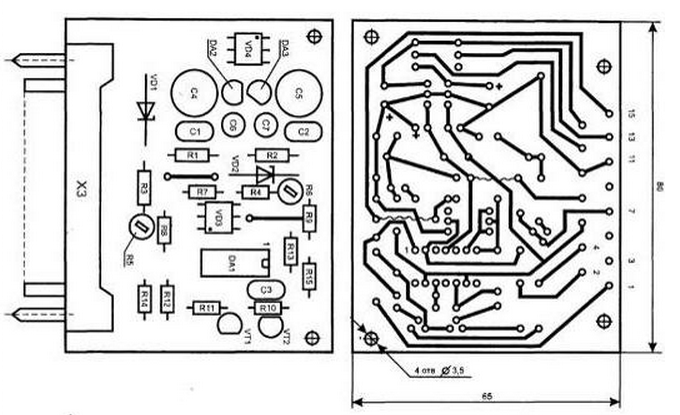
Fig. 4.11. A printed circuit Board, and the arrangement of the elements of the node A1
Node A2 can be performed surround installation and its dimensions depend on the type applied relay.
During Assembly used parts: a setup resistors R5 and R6 type SDR-19a; variable resistors R16.R18 type SPZ-4A or. PPB-1A; fixed resistors R19 C5-MV at 5 watts, and the rest from the IFL and S2-23 appropriate power.
Capacitors C1, C2, C3, C10 type K10-17, electrolytic C4…C9 type K50-35 (C50-32).
LEDs HL1, HL2 will fit any with a different color of illumination. Transistors VT1, VT2 can be replaced by CTA (B). Power transistor VT3 is set on the radiator area of about 1000 cm square Connector X3 on the Board. A1 type. RSN-2-15.
Relays K1, K2 applied Polish production is available for the R-15 with a coil on operating voltage 24 V coil resistance 430 Ohms) - they account for open-frame designs have small size and powerful enough switching the contacts.
Microammeter RA1 compact type M with internal or similar shunt current up to 3 or 5 A. For ease of operation of the power source circuit can be supplemented with a voltmeter that indicates the output voltage.
Mains transformer T1 is made independently on the basis of armour uniform industrial transformer with a capacity of 160 watts (for example, from series OSM TU16-717.137-83). The iron in place of the armature coil has section 40x32 mm. 'll Need to remove all of the secondary winding, leaving only network (if the primary winding is designed to 380 In it rewound 300 of turns). The start winding from the winding 8-9-10 - it contains 38+38 turns of wire. The PPP with a diameter of 0.23 mm. Winding 7-6-5-4-3 contains 16+15+15+15 turns of wire PEL with a diameter of 1.5 mm The secondary winding of the transformer must provide at idle voltage 18+18 V and 7,5+7,5+7,5+7,5 V, respectively.
With error-free installation in the scheme of the node A1 will only need to configure the maximum the adjustment range of output voltage 0…30 V resistor R5 and the maximum current protection 3 And resistor R6.
The switching unit (A2) does not require any adjustment. You only need to check the switching thresholds of the relays K1, K2 and corresponding increase in voltage at the capacitor C8.
When the operation of the circuit voltage green led lights (HL2), and the transition in the constant current mode, red (HL1).
To increase the maximum allowable current in the load up to 5 A in the diagram you will need to make changes as shown in Fig. 4.12 (set in parallel two power transistor). This is caused by the need to ensure reliable operation of the device in case of a short circuit on the output terminals.
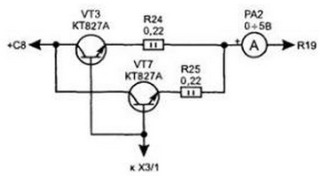
Fig. 4.12. The change in the scheme for the current in the load up to 5 A
In the worst case power transistors must withstand short-term overload power P=U I*I=35*5=175 watts. And one transistor CTA can dissipate an output not exceeding 125 W.
The switching voltage from the transformer T1 turnips K1 and K2 and inertial provide instant reduction in voltage coming from the secondary winding of T1, but they will reduce thermal power dissipation in the power transistors at continuous operation of the source.
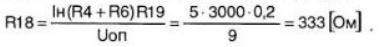
In the case of performing the power supply current is 5 And it is also necessary to reduce the value of the resistor R19 to 0.2 Ohms and with this in mind, to recalculate the values of the resistor R18 by the formula:
Author: I. P. Shelestov