


")

The power supply generates seven fixed values output voltage: 3, 5, 7, 9, 12, 18 and 24 or other that can be set, as desired, in the process of building. Its basis (Fig. 1) - pulse step-down regulator voltage, assembled on a chip DA1 and powerful field switching the transistor VT3. The control unit is applied to the chip. CKS (DA2), designed for use in devices selection of TV series USCT. It is a 8-channel switch, and upon filing with the buttons SB1-SB8 voltage on one of its inputs X1-X8 corresponding output (Y1-Y8) connected to the common wire. The state of the outputs of the chip shows the inclusion of one of LEDs HL1-HL8.
DA1 chip generates control pulses arriving at the gate of the transistor VT3, the duration of which depends on the voltage level at the inputs IN1. These inputs are used to control the output voltage the stabilizer. The voltage at the non-inverting input IN1 is supplied with voltage divider formed by resistors R23-R27 and R29-R31. Depending on the selected the output voltage control unit on the chip connects with DA2 General wire one of the resistors R23-R27, R30, R31, providing the required voltage the output of the power supply. The inverting input IN1 and IN2 receives voltage from resistive divider R14R16 connected to the output of built-in source reference voltage (VREF).
The switching regulator is fed from the feeding unit, harvested from the step-down the transformer T1, a diode bridge VD1-VD4 and smoothing capacitors C3, C4, and IC switch DA2 - parametric voltage regulator R11VD5C5.
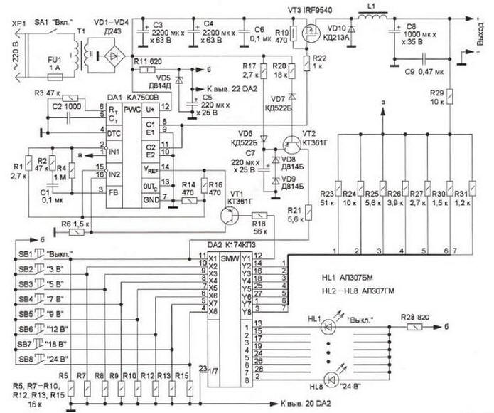
The signals arriving at the inputs IN2, control on and off the stabilizer. When you press the SB1 "Off" chip connects the right DA2 circuit output resistor R18 with the common wire. Transistor VT1 is opened and delivers the output voltage VREF circuits DA1 at its non-inverting input IN2. The voltage across it will be more than negated, the pulsed stabilizer will stop and the transistor VT3 is closed.
Chip DA2 together with the transistor VT2 protect the power supply from overload output current. When it occurs, the voltage at the rectifier output VD1-VD4 begins to fall, reducing the voltage on the base of transistor VT2. When it will be below the voltage charged on the capacitor C7, the transistor will open VT2, the voltage of the capacitor C7 will arrive at the input. X1 chip and DA2 will put the stabilizer in the Off state. Diode VD6 excludes discharge of the capacitor C7 through the resistor R17 and diode VD7 protects the transition the base-emitter of the transistor VT2 from the breakdown voltage of reverse polarity.
In the power supply applied to the resistors MLT, oxide capacitors - import, the rest K73-17. Diodes D243 you can replace any of the series D243-D, chip CAV - full analogue of the TL494. Buttons - any compact with momentary. The inductor is wound on two stacked rings of permalloy MP 140-4 size Chg. Coil contains 36 turns of wire. Sew-2 to 1.0. Before the winding of the wire rings are stacked together and wrapped with a layer of varnished cloth.
Diode VD10 and the transistor VT3 is set with the use of thermally conductive insulation strips for a total finned heat sink with dimensions 65x35x20 Buck mm. the transformer must provide an AC voltage at the secondary the winding 25…27 In load current up to 2.7 A. the device can be applied the transformer series. CCI, for example, TPP-127/220. In the manufacture or finished transformer should be remembered that, in any operating mode. the output voltage of the rectifier must not exceed 40 In - extremely allowable voltage stabilizer DA1.
Most of the parts and the heat sink is mounted on a circuit Board of one-sided foiled fiberglass, a drawing of which is shown in Fig. 2 and 3. Her the racks are fixed in a metal casing, there is mounted a transformer (Fig. 4). On the front panel set the buttons, LEDs, power switch, fuse holder and output jacks.
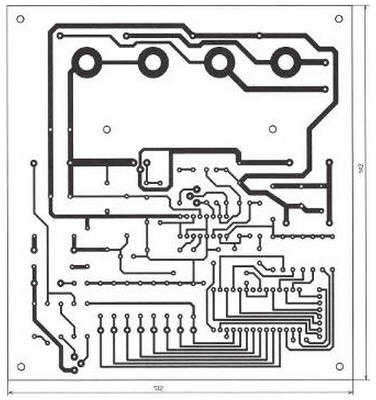
Fig. 2
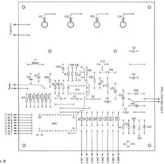
Fig. 3
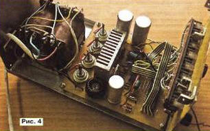
Fig. 4
The establishment of the device is reduced to the selection of resistors R23-R27, R30, R31 for accurate set the values of the output voltage. Work overload protection check, briefly closing the output of the supply, switch in the Off state. A short press on one of the buttons SB2-SB8 should restore the device.
Author: A. Abramovich