


")

Sorry scheme of the electronic device, every ham first tries in her work. Further, it is possible to make suitable device or (with experience) to make further improvements. And in fact, and in another if the required power source. You can buy it or win the lottery, but it is best to make with your own hands. In this lab ham will add the device not only basic, but useful functions.
For example, the power supply will try to trace the entire design process and manufacturing Amateur radio electronic devices.
The output voltage is constant. But with the amount it is necessary to understand. In mostly all of the circuit using a voltage of 12 V. However, chip CREW, like other circuits, can work with other the voltages. Therefore, in the power source for experimental work should to provide a wider range of output voltage. And better if it you will adjust.
Next, you need to resolve the issue, and what the limits to implement the change the output voltage?
Here it helps to know the chip CREW, which narrates this book. Minimum operational voltage is 3 V. the nominal voltage for most devices 12 V. Therefore, the power source must provide at the output voltage from 3 to 12 In? Let's not jump to conclusions, but let's look more widely. The necessary supply, especially since the chip allows you to work and when higher voltage (it can be up to 40 In). Also, if to experiment with chip CRAP, you may need not only voltage of 12 V, and up to 27 V.
But we will not venture on such a large value, and restrict the range the output voltage of our source from 3 to 15 V. this will be done food not only analog circuits, such as operational and low-frequency amplifiers, and digital circuits as TTL and CMOS.
Now we need to determine the load current. The majority of the considered devices consume a small current (about 10…50 mA). They can be powered from ready low-power adapters. However, we will not be limited to such current, and will do a device that can "grow", helplessly.
Having defined the main parameters output voltage of the power source, will deal with its structure, i.e. consider what the basic and auxiliary of nodes it needs to be.
Due to the fact that the source of electricity in our homes is a network alternating current, a source of increased danger, it is necessary decoupling a transformer. Also called power. He needed to pass (transformation) energy network. This is its main function. In addition, the transformer converts the high voltage (220 V) in low secondary (12…15).
But to power electronic devices require DC voltage and the desired corresponding inverter. So you will need a secondary rectifier AC voltage to DC. Pulsating voltage after the rectifier smoothed by the filter. The simplest filter is a conventional capacitor of a large capacity.
One part of the power source determined is a transformer, rectifier and a filter.
Due to the fact that the mains voltage is unstable, there are sharp jumps and slow changes, and it is unacceptable for electronic circuits, you will need the node providing a stable supply voltage. He called the stabilizer. As you know, they are impulse and linear. Given the scope of the experimental work in the power source must be able to adjust the output voltage.
As you might expect, in the process of prototyping and testing works are possible error, therefore, to protect the power supply and the load from dangerous modes of operation, it is necessary to provide protective measures. One such measure, which is most often used in electronics is a current limitation. In this case it is necessary to limit the load current, when exceeding or even a short circuit (short-circuit) not out of order (or even fired) power source. It is also desirable to have the ability to install a certain limit current limit.
A continuous overload of the power source, even if scheme protection. Therefore, it is necessary to have an additional node to the operational display (sound or light signal) dangerous regime.
Here we have determined the structure of the network is stable single-channel power supply with protection.
Enumerate the nodes:
- the network part - transformer, rectifier and filter;
- a voltage regulator;
- the node control voltage limitations in the load;
- node adjustable output voltage;
- the indicator voltage drop at the output.
The next task is to determine the components of our in the device. What elements and in what modes will be provided the main goal of our project is to provide the supply voltage for Amateur radio works.
The known chip type CREW in buck mode the stabilizer may well provide the required output parameters (3…12 V, 0,1…0,5 A).
Required to supply the load a few watts of power "pull" unified transformer type TP. It is designed for rated power 7.2 watts and is designed circuit Board. These transformers are manufactured on a range of output voltages and it is possible to choose the best one for our case.
The output voltage can be adjusted smoothly or stepwise. For convenience work selected stepwise method of the output voltage. Easy pressing the button - and always know the amount of voltage is applied to load. And as a switch (body temperature) is applicable button a partitioned switch type P2K.
Similarly construct the node limit of the load current. Applicable also stepped switching using P2K.
The acquired experience in the application of the chip CREW tells us that the indicator lowering of the output voltage is within the permissible limits can also design based on it.
Having defined the basic units and components of the projected source power, you can make it up the block diagram. The circuit shown in Fig. 5.14, it corresponds to our project.
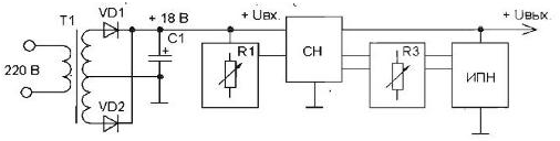
Fig. 5.14. Block diagram of the power source
Central to this scheme are network (dividing) with transformer full-wave rectifier and a filter and a voltage regulator (SN). On the output of the regulator is enabled indicator low voltage (IIT). Here there are also two management node: the current restrictions (R1) and weekends voltage (R3).
Developed a block diagram of a power source with the necessary functions for laboratory of radio sets and design features. After all the design of the power source must provide convenience when working with it. It is also necessary to ensure prompt repair when it fails.
Indeed, from a power source is required uptime and minimum time to recover after a loss of efficiency.
In this case, it is quite acceptable modular design of the device. Its peculiarity is that on a common circuit Board mounted transformer and capacitor filter (major elements) and other nodes (SN, IIT, etc.). Each of these nodes is on a separate circuit Board. If necessary each node can be disconnected from the total fee and repair. To obtain minimum total PCB construction sites should be located on General Board vertically. They can even be installed in special connectors.
To this the solution pushes that mode switching is performed switches LK. Once installed on the circuit Board, they seem to "lie" on it, occupying a large area. Therefore, with the location of the vertically P2K and press up will reduce the footprint on the General Board. So by the way, the volume of the device will be filled efficiently. The total fee will be minimum dimensions. And the size of boards of individual units will be determined on the one the parties shared channels (width), and on the other hand, the height of switches and P2K transformer (height).
In accordance with the structural diagram of our device on the main Board with transformer, rectifier and filter capacitor are installed:
- Board with chip buck stabilizer;
- Board with resistors limit the current and P2K;
- Board with resistors adjustable output voltage and P2K;
- Board with chip indicator lowering of the output voltage and the system.
To extend the functionality of a power source can be further to be installed on the card with the chip linear voltage regulator. This will allow to have a second voltage with independent adjustment. In addition, this output voltage will have a smaller pulse level which is necessary for working with sound-amplifying devices.
With that said, the total fee will be of the form shown in Fig. 5.15. Massive transformer connected to the interface Board by two screws, which provided mounting holes. In addition, the terminals of the windings of the transformer, soldered to the Board, also create additional mount.
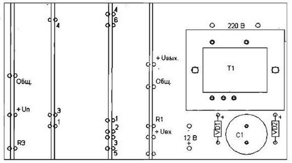
Fig. 5.15. The General layout and arrangement of elements on a common circuit Board laboratory power supply (right - network side of the transformer, to the left Plata indicator under voltage, charge regulating element current stress limits, the fee is partitioned resistors and fee stabilizer voltage).
If possible, the network connecting wire can be made using special contacts.
How is the network portion of the power source, it is clear from the diagram in Fig. 5.14. A scheme of the basic node of the voltage regulator (SN) is shown in Fig. 5.16.
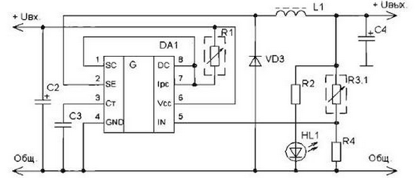
Fig. 5.16. An electrical pulse of a reducing stabilizer chip CREW.
SN made under the scheme buck stabilizer on the basis of chip CREW. Here conventionally shown that the permitted change in the magnitude current restrictions (R1) and output voltage regulation (R3).
The current limit or the maximum load current is set using the regulating element (R1). A detailed diagram of the switches and set resistors shown in Fig. 5.17.
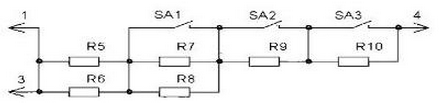
Fig. 5.17. The electric circuit of the regulating element current limiting load.
The electrical circuit consists of switches SA1-SA3<P2K) and resistors R5-R10. The feature of this scheme is that used all resistors same value (R = 1 Ohm).
The maximum load current (approximately 600 mA) for all closed switches, when the resistance R1 is 0.5 Ohms. Accordingly, the current is 300 mA (open loop SA1), 150 mA (at open SA1 and SA2), 100 mA (when open SA1, SA2 and SA3). The switches. P2K must have independent hold and then to press more than one button. There are other possible combinations of keystrokes that will fit other currents restrictions. The reader is invited to determine the additional value of the current restrictions.
It should be noted one feature. In the diagram there is a jumper 1-3. She designed for removal of hazardous mode during maintenance and when unidentified Board control voltage and random the supply voltage. As the jumper is connected in series in the input circuit of the stabilizer, in its absence fee buck stabilizer will be de-energized.
Adjusting the output voltage of the buck stabilizer is the resistor in the upper shoulder of the feedback divider (R3.1). He also performed on the switches P2K and resistors. The values of these resistors are designed so that the output voltage can be changed with a step of 1 V. to fewer details by selecting the ratio of the resistors (R13: R14 : R15 : R16) binary law: 1-2-A-8. Thus, using a partitioned resistor, the diagram of which is shown in Fig. 5.18, it is possible to set the magnitude of the upper shoulder divider as in SN and in IIT. In this case, the output voltage can to have a value from 3 to 18 In, because the resistance changes from 1.8 to 16.8 kω com (1.8 kOhm + 15 ohms).
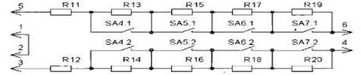
Fig. 5.18. The electric circuit Board partitioned resistors.
We should note that the diagram shows not only the divider for SN, but the divider for IIT. His work we will consider later. Jumper 1-2 for prevent dangerous mode of operation in the absence of the card with the dividers and random the supply voltage.
The accepted ratio of resistor values, and determines the appropriate work with the switches. For example, it is necessary to set the output voltage At 5 V. all closed switches (SA4, SA5, SA6 and SA7) the output should be 3 V. Therefore, it is necessary to add 5 - 3 = 2, i.e. SA5 must be open and R15 = 2 ohms in the circuit. Similarly installed and other necessary the voltage at the output.
Due to the fact that the switches are coupled, changes occur in the other the divider. It is designed to pit and similarly executed with the same the ratios of the resistors.
Consider the diagram of voltage droop at the output, which is shown in Fig. 5.19.
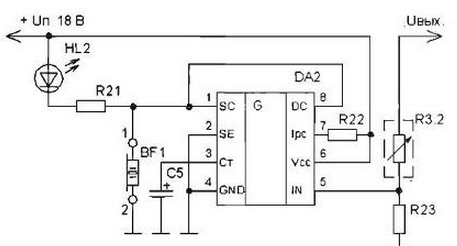
Fig. 5.19. The electrical circuit of the indicator voltage drop at the output the power source.
The main part of the indicator under voltage - chip CREW. She operates in the pulse generator. Briefly review the operation of this auxiliary diagnostic node.
Unstable power supply voltage comparator circuits compare ( pin 5), with a stable voltage reference. According the ratio of these voltages is the management of other nodes of the chip.
In the case where the voltage of the power source normal (potential output 5 exceeds 1.25 V), the comparator converts the output transistors non-conductive in state. The red led (HL2) is not lit.
When the voltage is switched comparator and starts to work the internal oscillator. The output transistors are alternately transferred from an open to closed, and periodically starts blinking red led. Current through it specifies the resistor R21, at the same time appears and the audio signal, since the piezo oscillator BF1 starting to click when switching transistors.
Thus, the electronic device is an indicator of lower voltages - continuously monitors the output voltage of the power source and draws attention light and sound signals when it is reduced in case of the overload. And this is possible in excess of the specified load current and the triggering of the protection circuit SN.
In addition, the indicator will be triggered in the absence of the output voltage at the output SN. Thus, if the repairs do not accidentally installed any charge with partitioned resistors (and the fee SN de-energized), then the alarm sound will bring them to your attention.
Intended functions are implemented and the layout of the laboratory power supply thought out. Now we have to design sites that are located on a separate the printed circuit boards and mounted on the main Board to the transformer.
Fee buck stabilizer (Fig. 5.20) is located closest to the rectifier. This reduces the length of conductors through which current flows load.
To reduce ripple and improve the stability of the stabilizer in addition to the main filter capacitor (C1) on this Board there the capacitor C2 (composed of two - C2' and C2"). Thus reduction of the dimensions of the Board. With one capacitor Board height would be more.
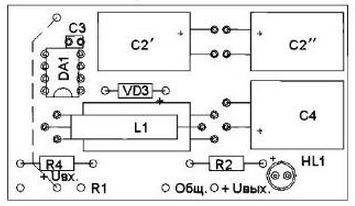
Fig. 5.20. The location of elements on Board switching regulator.
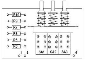
Fig. 5.21. The location of elements on the Board regulating the current element stress limits.
Another feature of the tab design is that the cumulative the filter choke is performed on a cylindrical compact unified the chokes DM type (PDM). To obtain the desired inductance provided series connection of up to 3 chokes DM type.
The indicator of the presence of the output voltage across the led HL1 can be installed on the front panel of the power source and connected to the pulse Board stabilizer wires.
Limit the load current is set using a partitioned resistor, located together with the switches on the Board as shown in Fig. 5.21.
The output voltage MV and the voltage response of IIT is set using partitioned switchable resistor, the details of which are on the Board, shown in Fig. 5.22.
The switches. P2K installed horizontally into the holes on the Board and their fixing screws are not, as by brazing. And the upper resistors shoulder divider mounted in hinged manner on the findings of P2K. Thus resistors each divider are arranged on different sides and connected to the Board wires.
And, finally, the General Board is another indicator voltage drop at the output SN and layout of which is shown in Fig. 5.23.
The piezo oscillator BF1 is soldered directly on the Board. Led HL2, indicating a dangerous mode of operation of the power source, can be installed on the front the side of the case and connect the wires to the Board.
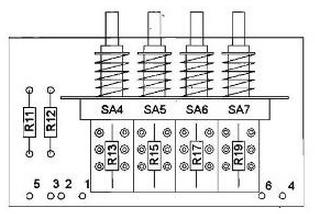
Fig. 5.22. The location of elements on Board switching regulator.
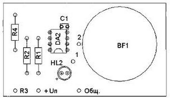
Fig. 5.23. The location of elements on the Board of the indicator voltage drop at output.
There are two options for fixing the PCB on a common circuit Board. First, on a common motherboard to install the connectors, specially designed for direct connection to printed circuit Board (SNP). Secondly (and this method easier), you can implement the consolidation of separate units vertically with staples from uninsulated about login Noah copper wire with a thickness of 0.8-1.0 mm. She soldered to the Board and is bent from two sides. And then all the staples installed in the opening of the total fee and is also soldered.
The obvious drawback of the second method: the permanent connection is not allows you to quickly disable the faulty node for repairs.
Despite its complexity, the first method (with connectors) is more suitable for advanced variant of laboratory power supply. If you want to add a regulated voltage output with low ripple, then it would require install another Board linear regulator. This may be the stabilizer a positive voltage. However, quite often you want a negative voltage, for example, to power the circuits of operational amplifiers. So still need a place to install the card with the chip stabilizer for a negative voltage. For convenience you can also use the installation fixed output voltages using partitioned resistors.
When thinking power with a limited set of functions, and then by gradually increasing modernization, and construction shall be provided appropriate opportunities.
Display of foresight in this matter and an increase in the size of the main Board to mount circuit boards additional components would help if you experience a corresponding requirement is relatively easy to modify the power source for increasing functions.
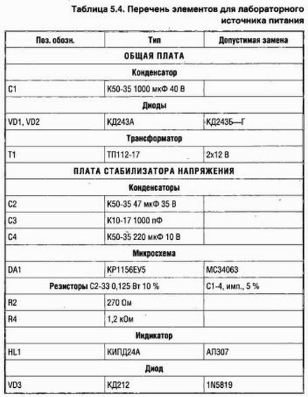
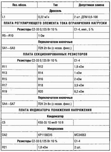
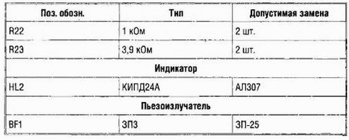
The manufacture of our options power source must begin with the selection required components. Their list is given in table. 5.4. Here you can find all the necessary radio components, but with the division on the boards of individual nodes.
The next stage of manufacture is the verification of all radioactive elements. When this condition will have the confidence that, after Assembly of the device earn, and will not have to waste time Troubleshooting because poor quality of components and facilitate their removal.
Of course, still necessary and the circuit Board. They are made of foil sided PCB thickness 1.5 mm for the sketches shown in Fig. 5.24-5.28.
The use of printed circuit boards facilitates the installation of radio components, but their fabrication associated with specific skills and the use of chemicals.
You can go on to another, cheaper and simpler way. Carefully looking closely to the conductors on the drawings sketches, printed circuit boards, it is possible to notice, the installation is simple and can be hinged manner. Moreover, this promotes, for example, the presence of hard conclusions from the transformer, switches P2K and other elements. They can be used for direct interconnection of elements and to secure installation of conductors.
After the mounting of the elements on the PCB must be carefully checked correct installation (especially polar components) and the quality of connections. Making sure there are no errors, you can proceed to the next stage of manufacturing the power source. He is in the Autonomous test each Board.
We should start with the total fee. Feeding the supply voltage to the primary winding transformer, it is necessary to measure the DC voltage across the filter capacitor.
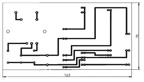
Fig. 5.24. A General sketch of the PCB transformer.
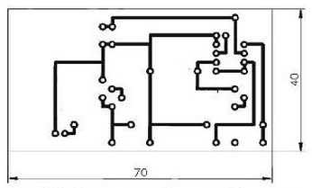
Fig. 5.25. A sketch of the circuit Board voltage regulator.
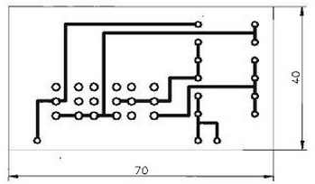
Fig. 5.26. A sketch of the circuit Board regulating element current limiting load.
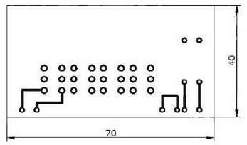
Fig. 5.27. A sketch of the PCB partitioned resistors.
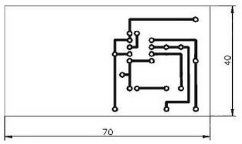
Fig. 5.28. Sketch a circuit Board indicator, low voltage.
Making sure that this part of the device is functioning correctly, it is necessary to produce another test under load. For this purpose, the output of the rectifier is connected to the resistor the value of 27 Ohms (2W) for providing load current of 0.4…0.6 A and again check the output voltage. Its value should be approximately 12 V.
After checking the normal operation of the card with the rectifier, it can be used for check the operation of the Board CH. However, before you submit the voltage on CH, you must put a jumper between the pins on the card connecting the terminals circuits 6 and 7, i.e. to exclude the resistor limits the current in the load (R1). More you must install a temporary divider output voltage (for backward communication). The resistor value is 6.8 ohms should be in place of the resistor R3.1 between the pin 5 of the chip and the output SN <Uвых).
After all these preparatory operations can apply the input voltage and to test the MV RH = 200 Ω, i.e. at small load currents (Ls - 40 mA). The power of this resistor should not be less than 0.5 watts. In this mode measure the output voltage of the SN, its value should be about V.
The next step is to check the stability of the output voltage when the load. For this purpose connected in parallel with the load resistor still the same (200 Ω), i.e. we get RH = 100 Ohms. In this case, the load current will double and will be about 80 mA. Measuring again the output voltage, you must ensure that it varies in accordance with the parameters of the chip and the whole unit works normally.
Now we have to check partitioned resistors. This can be done with using a DMM (digital multimeter). Make sure that when you the respective button, the total value of the resistor is measured by the device corresponds to included in the design, this motherboard can be set to General.
Further, similarly to the test Board with the resistors of the regulating element current stress limits (R5-R10) and also install it on a shared cost.
When the General Board will be established by all three boards: stabilizer voltage, partitioned dividers and regulating element current limiting load, we can proceed to the integrated audit of the functioning fully assembled without SSI network. This can be done using additional regulated power supply. For ease of check in as you can use the network portion of our power supply, but be aware that some settings (for example, stability voltage) cannot be checked.
Sequence verification of the collected power source as follows:
- the first thing you need to ensure that the output SN can be obtained all value of output voltage (with appropriate switches on Board of partitioned dividers) that were included in the design. It can be done with a multimeter and definitely under load (just 40…50 mA);
- next you need to check the protective properties of the SN. To do this, you must install using different limiting resistor maximum output currents and to increase the load until the output voltage starts to decrease. You must also make sure that the current limit occurs at the level which was laid;
- in conclusion, it is necessary to establish in its place visually verified cost indicator low voltage and verify that it starts to produce warning signals when reducing the output voltage;
- if desired, prior to operation of the power source can be more precisely adjusted (the selection of resistors) as output voltage and trigger voltage the indicator.
It now remains to strengthen the overall cost of collection inside the body and produce connection to output terminals.
Finally convinced that all parameters are OK, you can start to work with the power source.
Author: I. Koltsov L.