


")

The first problem with which when designing any device face and novice and experienced hams is a power supply problem. In this Chapter, will be considered a variety of network sources of power (Micropower, average power, powerful).
In the selection and development power source (hereinafter SP) it is necessary to consider a number of factors that are determined operating conditions, the properties of the load, security requirements and etc.
First of all, of course, you should pay attention to the conformity of the electrical parameters PI the requirements of the powered device, namely:
- the voltage
- supply current
- the desired level of stabilization of the supply voltage
- acceptable level ripple voltage.
Important characteristics of entrepreneurs, influencing its performance:
- the presence of protective systems
- weight the dimensions.
As an integral part of electronic equipment, means of secondary power shall be rigidly to meet certain requirements, which are defined as requirements the apparatus in General, and applicable to power sources and their work in the composition of this equipment. Any of the parameters PI, beyond the boundaries of the valid claims, brings discord into the operation of the device. Therefore, before you start Assembly on IE prospective design, carefully consider all the options available and select this IP, which will be best meet all the requirements and your abilities.
There are four main the type of network power supplies:
- transformerless, with the quenching resistor or capacitor
- linear, made by the classical scheme: step-down transformer - the rectifier - filter - regulator.
- secondary pulse: step-down transformer-filter - high-frequency Converter 20-400 kHz.
- pulsed high voltage high frequency: filter - rectifier AC 220 V - pulsed high-frequency
Converter 20-400 kHz. Linear power supplies differ utmost simplicity and reliability, the lack of high-frequency interference. High availability components and ease of fabrication makes them most attractive for repetition budding radiocontroller. In addition, in some cases, it is also important purely economic calculation - linear FE explicitly justified in devices that consume up to 500mA, which require a fairly small IE. These devices include:
- chargers for batteries;
- power supplies radios, caller ID, alarm systems, etc.
It should be noted that some designs that do not require galvanic isolation industrial the network can be fed through the quenching capacitor or a resistor, wherein current consumption may reach hundreds of mA.
Efficiency and the rationality of the use of linear PI is significantly reduced when the currents consumption of more than 1 A. the Reasons for this are the following phenomena:
- fluctuations network voltage affect the stabilization factor;
- at the entrance of the stabilizer you have to set the voltage, which will certainly be higher than the minimum valid at any fluctuations in voltage, which means that when these vibrations are high. it is necessary to set the voltage too high, which in its affects the pass transistor (unnecessarily large voltage drop at the transition, and as a consequence - high heat);
- a large current consumption requires the use of dimensional radiators on rectifying diodes and regulatory the transistor degrades the thermal regime and the dimensions of the device in General.
Simple enough in manufacturing and operation of secondary pulsed voltage converters, features ease of fabrication and low cost components. Economically and it is feasible to design a PI scheme secondary pulse Converter for devices with a current consumption of 1 to 5 And, for smooth on IE video surveillance systems and security for low-frequency amplifiers, radio stations, the chargers.
The best distinguishing feature secondary converters to line - weight features rectifier, filter, Converter, stabilizer. However, they are distinguished by a large noise, therefore, when designing it is necessary to pay attention to shielding and suppression of high frequency components in the power bus.
Recently received a fairly wide circulation pulse SP based high-frequency transducer with a transformerless input. These devices, eating commercial power supply-110V/220V, does not contain bulky low-frequency power transformers, and voltage conversion is high-frequency Converter at frequencies 20-400 kHz. Such power sources are on the order of the best massagana-ritimi indicators for compared to linear, and their efficiency can reach 90% or more. SP with pulse high-frequency Converter significantly improve many of the characteristics of devices powered by these sources, and can be used in almost any Amateur designs. However, they are distinguished by a high enough level the complexity, high level of noise in the power bus, low reliability, high the cost, inaccessibility of some components. Thus, it is necessary to have a very good reason for applying pulse SP based on high-frequency transducer in Amateur equipment (industrial devices is in most cases justified). Such bases can to serve: the probability of fluctuations in the input voltage in the range of ~100-300 V. the ability to create SP with power ranging from tens of watts to hundreds of kilowatts at any output voltage, the emergence of high-tech solutions available on the basis of IC and other modern components.
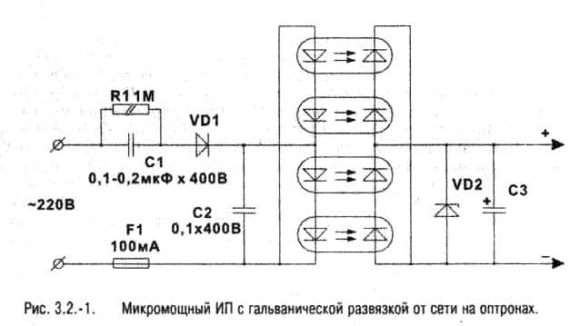
1. Power supply with galvanic isolation from the mains on the optocouplers
Micropower SP with galvanic isolation from the mains 220V (can be performed with the use of optocouplers, including them in series to increase output voltage (Fig. 3.2-1.). The energy transfer is performed by unidirectional luminous flux inside the optocoupler (optocoupler contains a light-emitting and the absorbing element), such by the way, a galvanic connection to the network does not occur.
On one optocoupler is allocated 0.5 to 0.7 for AOD. AD and 4-for AOT, AOT (tributary 0.2 mA). For ensure the required values of voltage and current of the opto-coupler included series or in parallel. As a buffer element of a sum you can use ultracapacitor, battery or capacity 100-1000 UF. LEDs are powered via a capacitance of less than 0.2 µf to avoid destruction. Need remember that the effectiveness of optocouplers declines over time (approximately 25% for 15,000 hours of work).
2. Micropower regulator with low consumption
In some Amateur designs are required Micropower stabilizers consuming in the stabilization mode microamperes. In Fig. 3.2-4 shows the schematic diagram such stabilizer with internal current consumption of 10 mA and a current stabilization 100 mA.
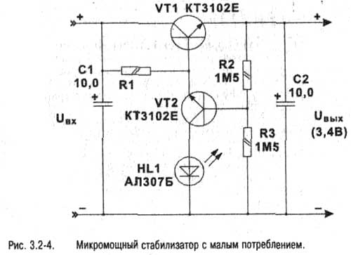
Indicated on the diagram elements of the voltage stabilization is Uвых=3.4, to change instead of HL1 led can be connected in series diodes KD522 (each the voltage drop is 0.7 In: transistors VT1, VT2 - 0.3 V). Input the voltage of this regulator (Uвх) up to 30 V. Should be applied transistors with maximum gain.
3. Power sources with a separation capacitors
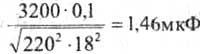
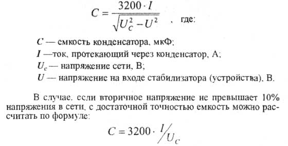
In a Micropower sources power supply with galvanic coupling with the industrial network is usually used so-called coupling capacitors, which are nothing like shunt resistance included in series in the supply circuit. You know, the capacitor is installed in an AC circuit that has a resistance, that depends on the frequency and is called reactive. The capacity of the separation capacitor (conditional use in an industrial network ~220 V, 50 Hz) be calculated by the following formula:

For example: charger device for Nickel-cadmium batteries 12V capacity of 1 A/h can be powered from the mains through a coupling capacitor. For Nickel-cadmium battery charging current is 10% of the nominal value, i.e. in our 100 mA case. Further, given the voltage drop across the regulator In about 3-5, we find that at the input of the charger it is necessary to provide a voltage of ~18 In at an operating current of 100 mA. Substituting these data, we get:
the first formula:
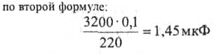
Thus, we choose C = 1,5 µf with twice the working voltage of 500 V (can be used capacitors types: MBM, IGBP, ILO).
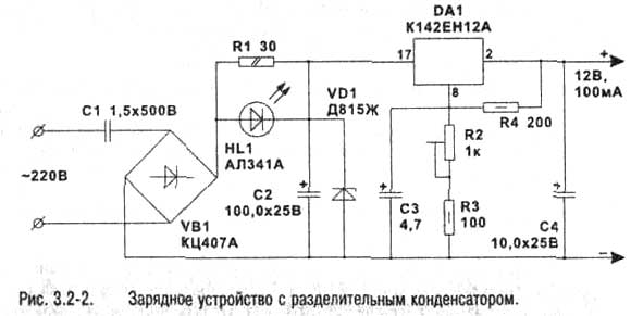
Full charging scheme device with a dividing capacitor shown in Fig. 3.2-2. Device suitable for charging current less than 100 mA when charging voltage no more than 15V. A trimming resistor R2 sets the desired value charge voltage. R1 acts as a current limiter in the beginning of the charge, and allocated to the voltage supplied to the led. The intensity of the illumination LEDs can be judged - as far as the discharged battery.

In the operation of this power source (and any other SP without galvanic isolation network) it is necessary to remember about the security measures. The device and charge the battery all time are at the potential of the industrial network. In some cases, such the restrictions make it impossible for normal operation of the device, so you have to provide galvanic isolation of FE from the network.
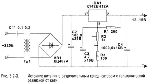
Low-power power source with the dividing capacitor, but electrically isolated from industrial the network can be made on the basis of the transition of the transformer or relay, magnetic starter, and their operating voltage may be below the 220 V. In Fig. 3.2-3 shows schematic diagram of the power source.
The capacity of the separation the condenser is calculated taking into account the parameters of the transformer (i.e. knowing the transformation ratio. first, calculate the voltage that must to provide for the input of the transformer, and then, convinced of the validity of such the voltage applied to the transformer, calculate the parameters capacitor).
The power delivered to such the power source may nourish the bell housing, receiver, audio player.

4. Power sources with a separation capacitors
In a Micropower sources power supply with galvanic coupling with the industrial network is usually used so-called coupling capacitors, which are nothing like shunt resistance included in series in the supply circuit. You know, the capacitor is installed in an AC circuit that has a resistance, that depends on the frequency and is called reactive. The capacity of the separation capacitor (conditional use in an industrial network ~220 V, 50 Hz) be calculated by the following formula:
For example: charger device for Nickel-cadmium batteries 12V capacity of 1 A/h can be powered from the mains through a coupling capacitor. For Nickel-cadmium battery charging current is 10% of the nominal value, i.e. in our 100 mA case. Further, given the voltage drop across the regulator In about 3-5, we find that at the input of the charger it is necessary to provide a voltage of ~18 In at an operating current of 100 mA. Substituting these data, we get:
the first formula:


Thus, we choose C = 1,5 µf with twice the working voltage of 500 V (can be used capacitors types: MBM, IGBP, ILO).
Full charging scheme device with a dividing capacitor shown in Fig. 3.2-2. Device suitable for charging current less than 100 mA when charging voltage no more than 15V. A trimming resistor R2 sets the desired value charge voltage. R1 acts as a current limiter in the beginning of the charge, and allocated to the voltage supplied to the led. The intensity of the illumination LEDs can be judged - as far as the discharged battery.
In the operation of this power source (and any other SP without galvanic isolation network) it is necessary to remember about the security measures. The device and charge the battery all time are at the potential of the industrial network. In some cases, such the restrictions make it impossible for normal operation of the device, so you have to provide galvanic isolation of FE from the network.
Low-power power source with the dividing capacitor, but electrically isolated from industrial the network can be made on the basis of the transition of the transformer or relay, magnetic starter, and their operating voltage may be below the 220 V. In Fig. 3.2-3 shows schematic diagram of the power source.
The capacity of the separation the condenser is calculated taking into account the parameters of the transformer (i.e. knowing the transformation ratio. first, calculate the voltage that must to provide for the input of the transformer, and then, convinced of the validity of such the voltage applied to the transformer, calculate the parameters capacitor).
The power delivered to such the power source may nourish the bell housing, receiver, audio player.
5. Linear power supplies
Currently traditional linear power supplies displaced by the pulse. However, despite this, they continue to be very convenient and practical solution in most cases, Amateur radio construction (sometimes in industrial devices). There are several reasons: first, linear sources power is structurally quite simple and easy to set up, and secondly, they do not require the use of expensive high-voltage components and, finally, they much more reliable than pulse SP.
Typical linear FE contains: mains step-down transformer, a diode bridge with filter and regulator, which converts the unregulated voltage derived from the secondary winding of the transformer through a diode bridge and filter in stabilized output voltage, and this output voltage is always below unstabilized input voltage stabilizer.
The main the disadvantage of this scheme is the low efficiency and the need for redundancy power in almost all elements of the device (i.e. installation required components allow greater loads than expected for FE in General, for example, for the SP 10 W required transformer capacity of not less than 15 W, etc.). The reason for this is the principle on which the function stabilizers linear IP. He is the dispersion on the control element some power Ppac = Nagr * (Uвх - Uвых) .From the formula it follows that the greater the difference between the input and output voltage, the greater the power you need to dissipate on the control element.
On the other hand, the more unstable input voltage stabilizer, and the more it depends on the change of the load current, the higher it should be in relation to the output voltage. Thus it can be seen that the stabilizers linear FE operate in a rather narrow scope of acceptable input voltages, and this framework is still narrowed at presentation strict requirements to the efficiency of the device. But achieved in a linear PI degree of stabilization and suppression of transient interference is far superior to the other schemes. Consider a few more used in linear FE stabilizers.
The simplest (so-called parametric) stabilizers based on the use of features the current-voltage characteristics of some semiconductor devices - mainly Zener. They are distinguished by a high output impedance. low level stabilization and low efficiency. Such stabilizers are used only for small loads, usually as a schema elements (for example, as sources of reference voltage). Examples of parametric stabilizers and the formula for calculating is shown in Fig. 3.3-1.
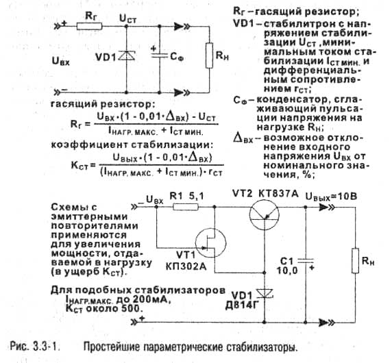
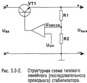
Serial passage linear regulators are distinguished by the following characteristics: voltage at the load does not depend on the input voltage and the load current, permitted high the value of the load current, high stabilization factor and small output impedance. Structural diagram of a typical linear regulator represented in Fig. 3.3-2. The basic principle on which he based his work - comparing the output voltage with a certain stable
reference voltage and management based on the results of this comparison, the main power element stabilizer (structural scheme-the so-called pass transistor VT1 working in the linear mode, but it may be a group of components), which dissipates excess power (see the above formula).
In most cases Amateur radio construction as sources of power devices can applied linear FE-based circuits linear stabilizers series K(CU)142. They have a very good parameters, have built-in protection circuit overload, temperature compensation circuit, etc., readily available and easy to the application (most of the stabilizers of this series is fully implemented within The IP that(have only three pins). However, when designing linear FE high power (25-100 watts) required a more subtle approach, namely the use of special transformers with armoured cores (having higher KDP), direct use only integral stabilizers is impossible due to failure of their power, i.e. need more power components and how the result, an additional chain of protection from overload, overheating and overvoltage. Such FE generate heat, involve the installation of many components on large heat sinks and, accordingly, a sufficient marker; achieving a high coefficient of output voltage stabilization is required special schematics.
6. Stabilizer with load current up to 5A
In Fig. 3.3-3 shows the basic scheme is to build a powerful stabilizers, providing the load current 5 A. what is sufficient for the nourishment of the majority of Amateur radio design. The scheme is executed with the use of chip stabilizer series CR and the external pass transistor.
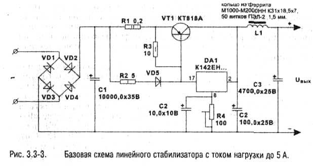
At low current consumption transistor VT1 is closed and only the chip stabilizer, but the increase in input current, voltage allocated to R2 and VD5, opens transistor VT1, and the main part of the load current begins to flow through his transition. The resistor R1 serves as a current sensor overload. The greater the resistance R1, the a less-current protection is triggered (the transistor VT1 is closed). Filter the inductor L 1 is used to suppress the pulsation of the alternating current at maximum load.
As shown in the diagram can to assemble the stabilizer to the voltage of 5-15 V. Power diodes VD1-VD4 should be with a current capacity of at least 10 A. the Resistor R4 is fine tuning output voltage (base value is set by the type of chips used stabilizer series KR). The power elements are mounted on radiators area of not less than 200 cm^2.
For example, let's consider the calculation voltage regulator with the following characteristics:
Uвых - 12;Nag - 3 A; Uвх 20 V.
Choose stabilizer voltage 12 V in series CR - CREB. Select the pass transistor, is able to dissipate the maximum power load RRAS = Uвх* Nagr = 20 • 3 = 60 W (power transistor, it is desirable to choose in 1.5-2 times greater) - fits common CTA (Rres = 100 W, IC max = 15). As VD1-VD5 can be any suitable current power diodes, for example,CDD.
7. Switching power supplies
Unlike traditional linear IC, involving the clearing of excessive unregulated voltage traversed a linear element, pulse SP use other methods and physical phenomena to generate a stabilized voltage, namely, the effect of the accumulation of energy in the inductors, and the possibility of high-frequency transformation and conversion of stored energy into a DC voltage. There are three typical schemes of constructing pulse SP (see Fig. 3.4-1): multiplying (output voltage higher than input), decreasing (output voltage below the input) and inverted (the output voltage is opposite in input polarity). As can be seen from the figure, they differ only the method of connection of the inductance, in other respects, the principle of operation remains unchanged, viz.
A key element (usually use of bipolar or MIS transistors), working with a frequency of about 20-100 kHz, periodically for a short time (not more than 50% of the time) is applied to the coil the full inductance of the input unregulated voltage. The pulse current. flowing through the coil, provides accumulation of stored energy in her magnetic field 1/2LI^2 on each pulse. Thus stored energy from the coil will be transmitted to the load (either directly, using a rectifying diode or through the secondary winding with the subsequent straightening), condenser the output of the smoothing filter provides a constant output voltage and current. Output voltage regulation is provided by the automatic adjustable width or pulse repetition rate on the key element (for tracking output voltage is the feedback circuit).
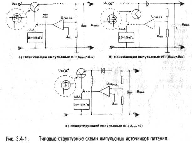
So, although quite complex, the scheme can significantly improve the efficiency of the entire device. The fact is what, in this case, in addition to the load in the circuit no power elements, scattering considerable power. Key transistors operate in the mode busy key (i.e. the voltage drop on them a little) and dissipate power only in a relatively short time intervals (the time of the pulse). In addition to this, by increasing the frequency conversion can be substantially increased power and improve overall dimensions.
Important technological the advantage of pulse SP is the possibility of building them on the basis compact network IP with galvanic isolation from the mains to power the a variety of equipment. These PIS are built without the use of bulky low frequency power transformer for high-frequency circuit the Converter. It is, in fact, the typical scheme of pulse SP lower voltage, where the input voltage rectified used network voltage, and as a savings element, the high frequency transformer (small-size and high efficiency), with the secondary winding of which is removed stabilized output voltage (this transformer also provides isolated from the network).
The disadvantages of pulse SP include: the presence of high level impulse noise at the output is high, the complexity and low reliability (especially in artisanal production), the need for expensive high voltage high frequency components, which in the case of any malfunction easily fail "all together" (in this case. generally, one can observe impressive pyrotechnic effects). Fans to dig into the internals of devices a screwdriver and a soldering iron when designing a network pulse SP will have to be extremely careful, as many of the elements of such schemes are under high voltage.
8. Efficient switching regulator low level complexity
On the base, similar used in the above described (Fig. 3.3-3) linear regulator, you can build a switching voltage regulator. With these characteristics it will have considerably smaller dimensions and better thermal regime. Schematic diagram of the stabilizer shown in Fig. 3.4-2. Stabilizer assembled according to the standard scheme with low voltages (Fig. 3.4-1A).
When you first turn when the capacitor C4 is discharged and is connected to the output powerful enough load current flows through the IC linear regulator DA1. Caused by this current drop the voltage on R1 key unlocks the transistor VT1, there also is included in the mode saturation, as the inductance L1 is high and through the transistor proceeds sufficiently high current. The voltage drop across R5 opens the main the key element is a transistor VT2. Current. increasing in L1, C4 charges, through feedback on R8 choking occurs stabilizer and key transistor. The energy stored in the coil that feeds the load. When the voltage on C4 drops below the voltage stabilization offer DA1 and key the transistor. The cycle repeats with a frequency of 20-30 kHz.
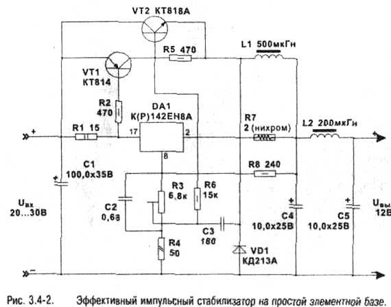
Circuit R3. R4, C2 will ask output voltage level. It can be adjusted continuously in small the extent from East DA1 to the Uвх. However, if Uвых to raise close to Uвх, appears some instability at maximum load and an increased level pulsation. To suppress high-frequency ripple at the output of the stabilizer an active filter L2, C5.
The scheme is quite simple and most effective for a given level of complexity. All power elements VT1, VT2, VD1, DA1 supplied with small radiators. Input voltage NS should to exceed 30 V. what is the maximum stabilizers KREN. Rectifier diodes to apply for a current of less than 3 A.
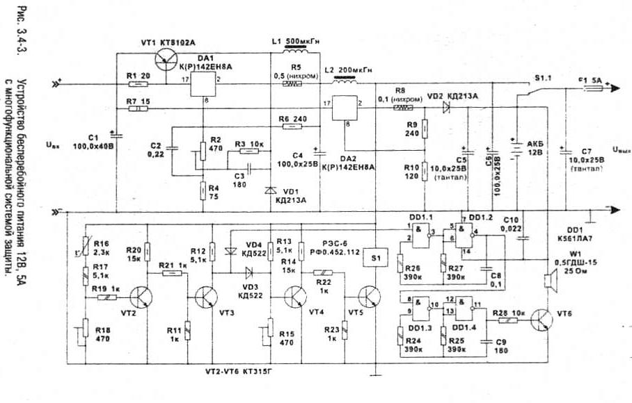
9. An uninterruptible power supply based on the pulse stabilizer
In Fig. 3.4-3 is proposed to review the device for uninterruptible power systems for the protection and video surveillance on the basis of the switching regulator, combined with a charging device. In the stabilizer system introduced protection against overload, over temperature, throws voltage output, short circuit protection.
The stabilizer has the following parameters:
- Input voltage, Uвx - 20-30 In:
- Output stable the voltage Uвыx-12B:
- Nominal current load AGR nom-5A;
- The current response system overload protection, SAS - 7A;.
- The voltage system surge protection, Uвых sett - 13 In;
- The maximum charging current Battery, SAR battery-max - 0.7 A;
- The level of pulsation. You need to open - 100 mV,
- The temperature of activation system overheating protection, Tsas 120 s;
- The speed switch on powered by battery, tперекл - 10ms (relay RES-b RIF.452.112).
The principle of pulsed stabilizer in the described device is the same as that of the stabilizer, presented above.
The unit completed charger, performed on the elements of DA2,R7, R8, R9, R10, VD2, C7. IP voltage regulator DA2 divider current at R7. R8 limits maximum initial charge current, the divider R9, R10 sets the output voltage charge, diode VD2 protects the battery from discharge in the absence of voltage power.
Protection against overheating uses as a temperature sensor PTC resistor R16. When triggered the protection is activated audible signal, assembled on the IP DD 1 and, simultaneously, the load is disconnected from the stabilizer, turning on the power from the battery. Thermistor mounted on the radiator of the transistor VT1. Precise adjustment of the trigger level thermal protection is implemented by the resistance R18.
The voltage sensor is assembled on the divider R13,R15. resistance R15 set the trigger level overvoltage protection (13). When exceeding the voltage at the output stabilizer (in case of the latter out of operation) relay S1 disconnects the load from the regulator and connect it to the battery. In the event of a power supply voltage relay S1 goes into the "default" meaning that connects the load on the battery.
The diagram is not has electronic protection against short-circuit to the battery. this role performs the fuse in the power supply circuit of the load, designed for maximum current consumption.
10. Power sources based on high-frequency pulse Converter
Quite often when constructing devices arise strict requirements to the size of the source power. In this case, the only solution is the use of IP-based high voltage high frequency switching converters. connecting to the network ~220 V without the use of dimensional low-frequency step-down transformer and can provide more power at small sizes and the heat transfer.
Structural scheme of the model pulse Converter powered industrial network presented in figure 34-4.
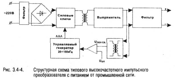
The input filter is designed to prevent the penetration of impulse noise in the network. Power keys supply high voltage pulses to the primary winding high-frequency transformer (can be used one - and two-stroke diagram). Frequency and the pulse duration are set by managed generator (typically used the control pulse-width, at least - frequency). Unlike transformers a sinusoidal signal of low frequency, pulse SP applied broadband device that provides efficient power transfer to signals with fast edges. This imposes significant requirements on the type the applied magnetic circuit and transformer design.
On the other hand, with increased frequency of required dimensions of the transformer (with privacy capacity) decrease (modern materials allow you to build a powerful transformers with an acceptable efficiency for frequencies up to 100-400 kHz). Feature the output of the rectifier is the use of it is not conventional power diodes, and high-speed Schottky diodes due to the high frequency rectified voltage. Output filter smooths the output voltage ripple. The feedback voltage is compared with a reference voltage and then controls a generator. Note the presence of galvanic isolation in the circuit feedback that is necessary if we want to ensure the isolation of the output voltage to the network.
In the manufacture of IE there are serious requirements components used (which increases their the cost compared to traditional). First, it concerns working voltage rectifier diodes, filter capacitors and transistors key, which must not be less than 350 To avoid breakouts. Secondly, should apply high-frequency transistors key (operating frequency of 20-100 kHz) and special ceramic capacitors (conventional oxide electrolytes at high frequencies will overheat due to their high inductance). And third, the frequency of high-frequency transformer saturation, depending on the type used Manitoba water (typically toroidal cores) should be considerably higher than the operating frequency of the Converter.
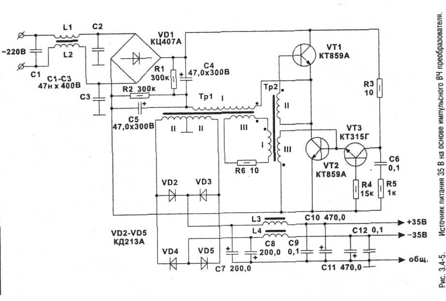
In Fig. 3.4-5 shows a schematic diagram of a classical FE-based high-frequency the Converter. The filter consisting of the capacitances C1, C2, NW and chokes L1, L2, serves to protect the mains from high frequency interference from the Converter. The generator is built in a self-oscillating circuit and combined with key stage. Key transistors VT1 and VT2 are in antiphase, opening and closing turns. The oscillator start-up and reliable operation provides the transistor VT3 operating in the avalanche mode. When the build-up of voltage on C6 through R3, the transistor opens and the capacitor discharged to the base VT2, starting the generator. The feedback voltage removed with additional (III) winding of the power transformer Tpl.
Transistors VT1. VT2 mounted on the plate, the radiator is less than 100 cm^2. Diodes VD2-VD5 with the Schottky barrier is placed on a small radiator 5 cm^2.
These chokes and transformers:L1-1. L2 is wound on the rings of ferrite 2000NM CHH in two wire wire PELSHO of 0.25: 20 turns. TP1 - two rings stacked together, ferrite N KZ 1x18.5x7; winding 1 - 82-loop wire sew-2 0,5: winding II - 25+25 turns of wire sew-2 1,0: winding III - 2 loop wire sew-2 0.3. TP2 is wound on the ring of ferrite NN CHH. all windings are made wire sew-2 0.3: winding 1 - 10 of turns of the windings II and III 6 windings, the two windings (II and III) wound so that is on the ring by 50% the square without touching or overlapping each other, winding I is wound uniformly on all over the ring and insulated with a layer of varnished cloth. Coil filter rectifier L3, L4 wound on the ferrite TO 2000NM HH wire sew-2 to 1.0, the number of turns - 30. As a key transistors VT1, VT2 can be applied CTA. CT, CT.
The values of elements and winding data transformers are given for the output voltage of 35 V. In when we need other work settings, matching the following major points to change the number of turns in coil 2 TP1.
The described scheme has significant disadvantages, driven by the desire to reduce the maximum the number of used components Is low "level output stabilization voltage, unreliable and unstable work, and low output current. However, it quite suitable for the nutrition of the simplest designs of different capacity (at the application of the relevant components), such as calculators. The caller ID. lighting devices, etc.
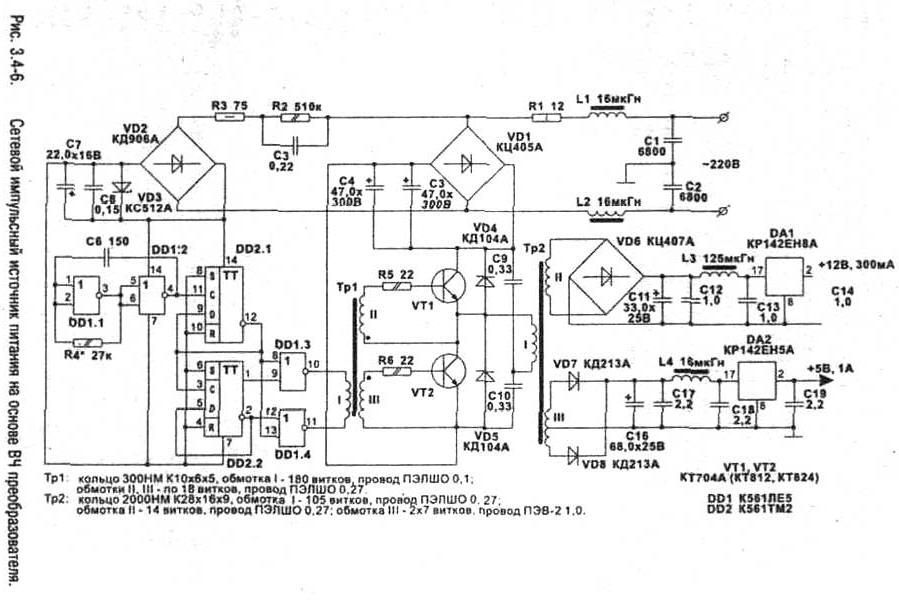
Another scheme of FE-based high frequency switching Converter shown in Fig. 3.4-6. The main the difference of this circuit from the standard structure shown in Fig. 3 .4-4 is the lack of the feedback circuit. In this regard, voltage stability the output winding of the HF transformer TP2 is quite low and requires the use of secondary stabilizers (in the scheme uses universal integrated stabilizers on the IP series KR).
11. Switching regulator with key MIS transistor with reading current
Miniaturization and increase Efficiency in the development and design of switching power supplies favors the application of a new class of semiconductor inverters - MIS transistors, and also: powerful diodes with fast reverse recovery diodes, Schottky, ultrafast diodes, field-effect transistors with insulated gate, integrated circuits control key elements. All these items are available for the domestic market and can be used in the fabrication of highly efficient power supplies, converters, systems ignition engines internal combustion (LWС), systems start fluorescent lamps (LDS). Great interest developers can also cause a class of power devices called HEXSense - MIS transistors with current sensing. They are the ideal switching elements for switching power supplies with ready control. The ability to read the current of the switching transistor can be used in pulse SP for current feedback required for the controller pulse width modulation. This is achieved by simplifying the design of the power source is an exception current resistors and transformers.
In Fig. 3.4-7 shows diagram of the pulsed power supply 230 watts. His main work the characteristics are as follows:
- Input voltage:-110 In 60Hz:
- Output voltage: 48 V permanent:
- Load current: 4.8 And:
- Switching frequency: 110 kHz:
- Efficiency at full load: 78%;
- Efficiency at 1/3 load: 83%.
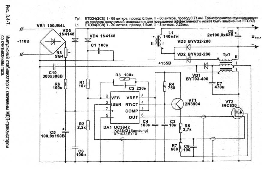
The scheme is built on the basis of the pulse width modulator (PWM) Converter with high frequency on output. The principle of operation is as follows.
The control signal key the transistor is supplied with 6 output PWM controller DA1, the fill factor limited to 50% resistor R4, R4 and NW are time-setting elements of the generator. Food DA1 is provided by a chain VD5, C5, C6, R6. Resistor R6 is designed to supply voltage during startup of the generator, subsequent uses feedback voltage across L1, VD5. This feedback is obtained from the secondary winding of the output inductor, which works in reverse mode. In addition to the power generator, the voltage reverse connection through a chain VD4, Cl, Rl, R2 is input to feedback voltage DA1 (pin.2). Through R3 and C2 are compensated, which guarantees stability of the closed loop.
As a key element VT2 is used MIS transistor with current sensing IRC830 company International Rectifier. The read signal current is supplied from VT2 to pin 3 DA1. The voltage level at the output of the read current is set by resistor R7 and proportional to the current flow, C9 suppresses emissions at the forefront of the current pulse. runoff that can cause premature actuation of the controller. VT1 and R5 used to set the desired control law. Please note that current read is returned in the crystal at the output of the source. This is done so. to avoid the error of the read current, which may occur due to the fall the voltage on the parasitic resistance of the output source.
On the basis of the scheme you can build a switching regulator and other output parameters.
12. Modern gas-discharge devices
Approximately 25% of the electricity produced in the world is consumed by artificial lighting systems that makes this area extremely attractive for application of forces in the field increasing the efficiency and reducing consumption the electricity.
Currently, the most common economical light sources gas-discharge lamp, are increasingly used instead of conventional incandescent bulbs. The principle of operation such lamps is in the luminescent glow of the prisoner gas inside the lamp when the flow of current through it (the implementation of high-voltage breakdown) is provided by applying a high voltage to the electrodes of the lamp. Discharge lamps can be divided into two types, the first is light, high intensity glow, among which the most common are: mercury lamps, sodium lamps high pressure metal halide lamp, a second type fluorescent low pressure lamps.
Low pressure lamps used for lighting in most cases, daily life - in administrative buildings, offices, residential buildings: they are characterized by intense white light. close to daylight (hence the name - "fluorescent lights"). Lamp high pressure is used for outside lighting - street lights the floodlights, etc.
If a standard bulb filament, when enabled, is a constant resistive load, all discharge lamps have a negative impedance characteristics. which require a constant current. In addition, it is necessary consider things such as: resonant mode of operation, protection at the exit of the tube failure; high voltage ignition, special control power bus. Basic mode, the observance of which is necessary for the fluorescent lamp on throughout the term exploitation is a current mode (ideally needed stabilization of power throughout the period of operation of the lamp). As a rule, the lamps are powered from AC voltage to equalize the wear of the electrodes (in the case of supply of constant voltage, the service life shorter by 50%).
13. Magnetic and electronic ballasts
To manage gas discharge lamps have traditionally been used so-called magnetic ballast (see the scheme in Fig. 3.5-1), however, due to its inefficiency and unreliability, recently becoming more common get the schema of electronic control - electronic ballast, which allows to significantly improve the efficiency and service life of lighting systems, make the light more smooth and natural to the eye.
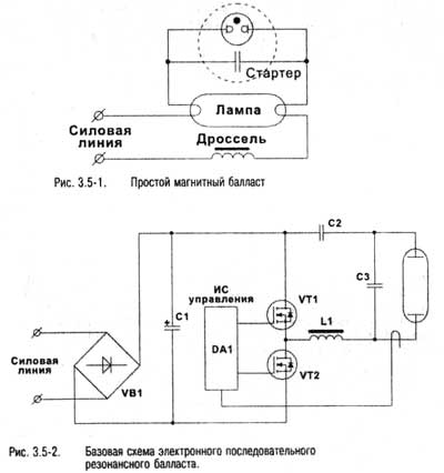
Basic diagram of the electronic ballast with a serial resonance is shown in Fig. 3.5-2. Applying electronic ballasts, you can control the lamps in any capacity, in the scheme can embed any additional devices (for example, photoelectric, including lighting at dusk and off at dawn).
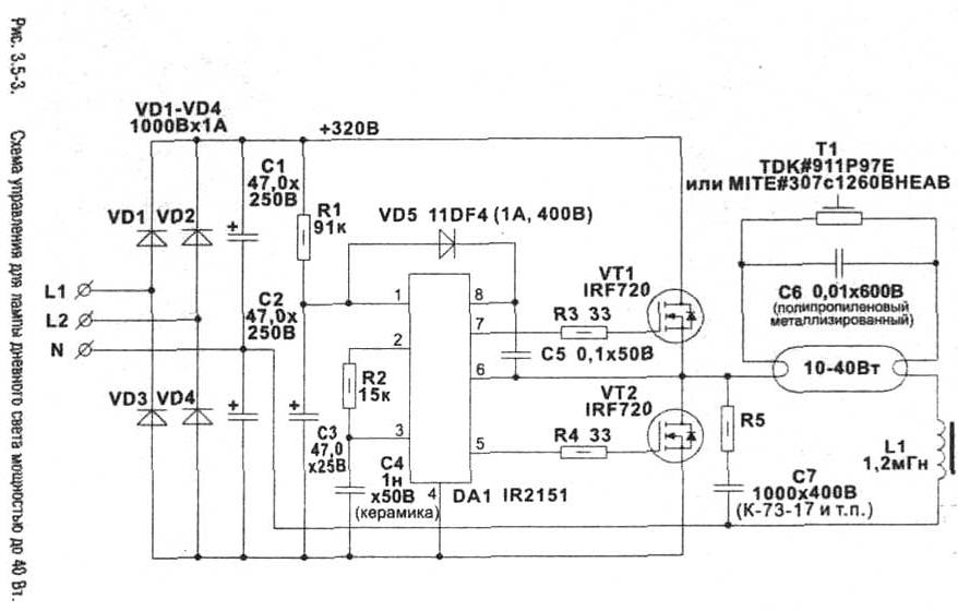
14. The control circuit for a fluorescent lamp power up to 40W
To control the lamp daylight (LDS) power up to 40 watts, use the circuit shown in Fig. 3.5-3.
Voltage ~220V served on L1 and L2. Rectified by diodes VD1-VD4 constant voltage is about 320 V. the Capacitors C1 and C2 operate as capacitive input a filter. Use network ~110V, in this case, power is supplied to L1 (L2) and N. and the diodes VD1. VD3 (VD2, VD4) with capacitors C1 and C2 are as the half-wave voltage doubler.
DA1 (IR2151) - this scheme control MOS-transistors with internal generator that works right from the power bus through R1. Internal stabilizer locks the voltage at the level of V. 15 is Provided to lock the gates when the supply voltage drop below 9 V.
At rated DC the voltage of the power bus 230 To output a rectangular pulse has an effective the voltage of 160 V and the frequency is set by the selection of R2 and C4 for the approximation to the resonant frequency of the lamp. Lamp works in his series resonant a circuit consisting of series-connected inductors L1 and shunt capacitor C6, which is in parallel with thermistor a positive temperature coefficient.
Thermistor (for these purposes can also be used a neon bulb) has a small resistance in cold and very high hot when heated due to the flowing current. The purpose of the thermistor is to provide a smooth the build-up of voltage on the electrodes of the lamp when turned on. In cases when the lamp is lit constantly or very rarely turns on/off, the thermistor can be removed. In this case, the lamp turns on instantly, which can to cause rapid wear.
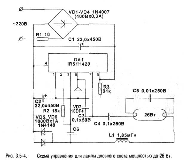
15. Subminiature control circuit for fluorescent lamps power up to 26W
This principle the circuit shown in Fig. 3.5-4, allows you to control a fluorescent light (LDS), while having a subminiature size, since it does not apply power inverters (IP IR51H420 combines in one case the IP and IR2151 TIR-keys). The maximum power of the lamp in this case should not exceed 26 W, which is enough to illuminate a single workplace.
16. Step-up converters and voltage multipliers
Usually, if the design there is a utility power, for all power supply use the transformers. Step-up converters and voltage multipliers are used, when you must obtain a voltage greater than the voltage in wearable devices powered by batteries or accumulators. Transducers low power (up to 100-200 mW) can be collected on discrete elements without the use of transformers, converters in a large power transformer is required. To obtain the doubled or trebled voltage it is possible to use so-called the voltage multipliers (see Chapter 2).
17. A transformerless voltage doubler for small devices
In Fig. 3.6-1 shows Converter circuit voltage 9 V -> 18V for devices that consume not more than 100 mA at a voltage of 18V. The Converter is provided as part practical schemes siren for security systems and alarm systems.
Generator control performed according to the standard scheme. D 1.2 formed rectangular pulses with a frequency of 1 Hz. The pulses arrive at a controllable oscillator Dl.3, D1.4 and chain from R3, R2, C2, which affects the depth of the modulation. R4, R5, NW, C4 are selected in accordance with a resonant frequency of the piezo ceramic emitter 1 in the range of 1.5-3 kHz. To increase the amplitude of the piezoelectric crystal in the scheme introduced the multiplier. The output signal DD1.4 is supplied to a complementary pair VT5, VT6 and further to the multiplier VD3, VD4, C5, Sat. The voltage on C6 with a load current of 50 mA and the main power supply 9 is In the order of 16 V. the Power of the multiplier can slightly increased by the capacity of the higher denominations. The circuit can be powered voltage 6-15 In (15 V maximum for the IP series 561), in the case of a 15 V power supply, the output voltage of the multiplier will be less than 25 NS In with a load of 80 mA.
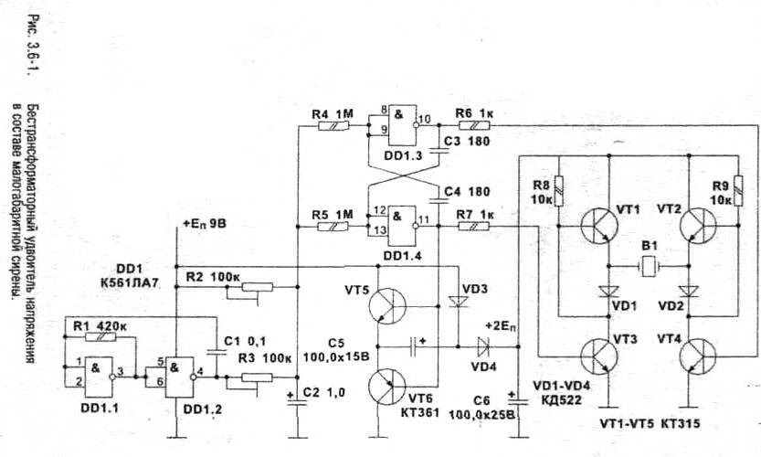
In this design
the amplitude of the crystal piezoelement that will be quadrupled, given the fact that he
included in antiphase relative to the shoulders of transistors VT1, VT3. As
the unit uses specially developed for these purposes ceramic
plate with double-sided coating, the so-called trimorph with the diameter of the crystal
32 mm.
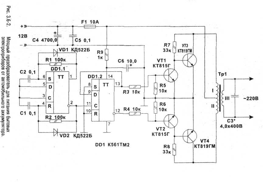
18. A powerful Converter to power household appliances
In Fig. 3.6-2 shows a schematic diagram of a power Converter to power household appliances (TV, drill, pump, etc.) from a car battery. The Converter provides an output voltage of 220 V, 50 Hz load power up to 100 watts. At maximum load consumption from the battery current does not exceed 10 A.
The amount of detail in the device is minimized. On the chip DD1.1 is assembled master oscillator with a frequency of 100 Hz. Fine tune the frequency (which is important for normal operation equipment) is performed by resistors R1 and R2. Divide-by-2 frequency and management the transistors are provided with the second half of the chip - D1.2. Transistors VT1, VT2 are included to ensure the normal operation mode outputs DD1.2 when maximum load current. The output transistors VT3, VT4 are installed on radiators, the area is not less than 350 cm^2.
For smoothing rectangular fronts designed capacitor NW, which together with the output winding and the load forms a resonant system. Its capacity is highly dependent on nature of the load. Transformer TR1 is made on Manitoba water mark or SLM PLA overall power 100 watts. The windings I and II contain 17 turns of wire Sew-2 2.0 mm, winding III contains 750 turns of wire sew-2 0.7 mm.
This scheme is very easy to be adjusted to the high-voltage Converter (frequency conversion ~25 kHz). It's enough to raise the frequency setpoint the generator D1.1 to -50 kHz by changing the capacitance C1 and C2 180 pF, and replace TP1 at high frequency transformer. The capacity of the transformer depends on the load the output transistors, the maximum current that they can give the national Assembly should to exceed 8A in the shoulder. To increase the current decreases the number of turns the transformer windings 1 and II to 8-10. At the Converter output installed a diode bridge and high-pass filter used in these components must to ensure the normal operation at a frequency of 25 kHz.
19. Protection against excessive mains voltage
In industrial and domestic network rather you can often fix the unexpected throws voltage, the voltage in the network may exceed the rated 20-40%. Such casts can conditionally be divided into two classes:
1. Short - term increase in the amplitude within a few periods.
2. Long - increase voltage in a few seconds or minutes.
The first can be attributed more to a pulse interference due to the switching at the line of some powerful loads (welding machines, motors, heating elements). They will certainly have impact on household appliances and especially on sensitive elements sources power TVs, stereos. which are often in standby mode round the clock.
20. The protection device pulse interference in the network
A device that protects against pulse interference shown in Fig. 3.7-1. The scheme consists of the following components:
- power source - VD1-VD4, R6, R7, VD5, VD7,Cl, C2;
- sensor-comparator - Rl, R2, R3, R4, R5, HL1, VD8, DA1, R8, R9;
- driver reset delay the off - VD9, R10, DD1.1,DD1.2, VD10, R11, NW;
- the pulse generator of high frequency 25 kHz to control timestorm-DD 1.3, DD1.4, R 12, R 13, C4, C5, R14, TP1, VS1.
- sounder (optional) - R14, R15, C6,C7,HA1,DD2.
The power supply produces two voltage: +24 V - for power pulse transformer +5V to power The IP device.
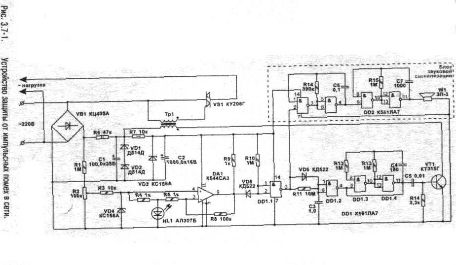
The node voltage control is assembled on Rl, R2, R3. With the voltage divider is input to the comparator. Level tripping over-voltage set resistor R2 (position engine is selected so that the comparator was on the verge of firing with 245 In the input). If exceeded, the comparator input of specified amplitude the values he switched and the output rectangular pulses appear with frequency of 25 Hz.
In the initial state at the output of D1.2 maintained a high logic level, allowing the operation of the generator management timestorm (to keep open). Transistor VT1 controls pulse transformer. forming powerful pulses of voltage open. The oscillator frequency is chosen equal to 25 kHz for the early release power key moments in the transition through zero (if the control frequency will be insufficient, it may happen that when during power-up will appear high-voltage release and will be distorted form a sinusoidal signal, the system will not have time to react and the distorted signal is sent to the load).
Differentiating the chain on the elements D1.1 and D1.2 performs the prohibition of operation of the generator upon receipt of the low level with the comparator output (while increasing the threshold voltage in the network) and with a delay in 9c allows you to run the generator when the voltage drops to the threshold the values of 240 V.
Pulse transformer TR1 is wound on Manitoba water size CHH,5 ferrite 2000nn and contains: winding I - 100 turns, winding II - 40 turns of wire PELSHO-0,22. Winding isolated from the ring with a layer of varnished cloth and placed on opposite sides of the ring.
When the power load is more than 300W simister must be installed on the radiator.
Publication: www.cxem.net