


")

Selectors, the principle of which is based on the synthesis frequency, called selectors PLL ("Phase Locked Loop", which translated to English means "closed loop PLL"). These selectors are also called digital because they are managed by the processor of the TV via a two-wire bidirectional digital the I2C bus.
Frequency synthesis significantly improves the accuracy of the settings on the TV station, simplifies the use of a TV, while still permitting manual adjustment to obtain optimal image quality [1 - 4].
Before proceeding to the description of selectors, let's explain some terms and conventions conventions for selectors PLL.
The flow of information via digital I2C bus can be transferred in two directions: from processor and to the processor. When it is directed from the processor to the selector (for example, the installation command), this mode is called the ENTRY. Postback the flow of information (from selector) corresponds to the READING mode, which set when the selector at some point informs the processor about its condition or confirms previously established (upon request of the processor). This mode are not all selectors PLL.
Further designations are used: AS (address Select) - address bus: SDA - serial bus data; SCL (Clock Select) - bus synchronization clock pulses; LW - voltage synthesizer (+5); ADC - five-level ADC, built-in synthesizer that enables you to manage any additional device through the selector.
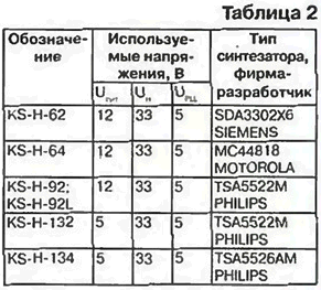
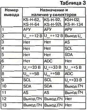
In table. 1 to 3 show the most important information on selectors PLL production JSC "SELTEKA" (Kaunas. Lithuania) [5] and their analogues - available modern selectors foreign firms (domestic models, unfortunately, are still not implemented in serial production). Other General information about them and the options were published in [1]. Recall that they are all - all-wave models European unification. Antenna input - type IEC (SNIR), if output - symmetric. In table. 2 and 3 UN - tuning voltage; pin 1 is closest to the antenna input. I selectors KS-H-132. KS-H-134 has only 11 pins. In these selectors supply voltage is +5 V and special output for voltage UPLL not provided, but there is an output voltage settings (0,5…28 V) - UH which facilitates the control of the selectors and allows manual the adjustment.
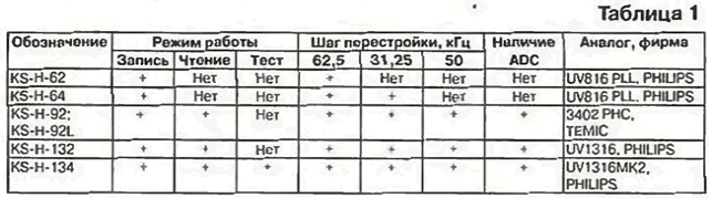
The simplest model - KS-H-62. The speed of adjustment, starting frequency 132 MHz sub-band A, 356 MHz sub-band In and 678 MHz sub-band, change (programmatically). to compensate for the nonlinearity of the dependence the capacitance of the varactors of the voltage settings.
In the selector KS-H-64 the speed of adjustment to changes in software. Itself the program is hardcoded in the processor.
KS-H-92 is a more advanced and complex selector. The speed of adjustment slows down (slightly - slightly) near TV stations to reduce the residual detuning. In tables are given parameters of the modernized (in late 1998) version of the selector KS-H-92, which installed the chip TSA5522M PHILIPS instead synthesizer company MOTOROLA. This option has become the equivalent of the selector RS company TEMS.
The selector KS-H-92L - variant KS-H-92 with an extended antenna input (32.2 mm). Similar functionality has the selector KS-H-132, but low supply voltage.
The new selector today can be called KS-H-134 (development 1998). In it changed the boundaries of the sub-bands of the received frequencies: A - C essential channel 1 on cable channel SK6 (47… 158 MHz). In - SC no SC (158…438 MHz); C - C S on 69-th channel (438…862 MHz). Introduced mode testing and changing the speed of adjustment is automatic. When the circuit loop of PLL (in the capture bandwidth of the channel) is provided switching speed of adjustment, and in the absence of fixation - return the speed change. Software enable/disable function speed adjustment allows you to switch to manual tuning.
In Fig. 1 is a block diagram of the PLL selector (on the example of the KS-H-92). It consists of three identical channels separation, amplification and conversion of signal. Each channel is designed to operate in only one sub-band (A, b or C). Consider the construction of one channel, for example, for sub-band A.
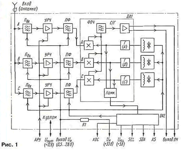
The radio signal from the antenna input is allocated to the input circuit, performing the role a bandpass filter (PM). and pass a radio frequency amplifier (RF amplifier). assembled a field effect transistor. Loading RF amplifier serves as a bandpass filter (PF). Input circuit and a bandpass filter rebuilt the varactors. Amplified signal the chip DA1 containing three separate balanced mixer-local oscillator (C/G). The contours of the local oscillators are also rebuilt the varactors. The if signal outstanding bandpass filter (FPC) and after matching of the cascade comes on output terminals of the selector (if output).
The lo signal through the switch (Comm) is supplied to the synthesizer chip frequency DA2. In Fig. 2 shows a partial structural diagram of the synthesizer, in which includes a model generator (DG) frequency Fo, the first programmable divider (PD) with a division ratio and To a second programmable divider (PD) the division ratio N, the frequency-phase detector (PD) and active filter bottom frequency, which is used as the integrator (And). The latter is not included in the composition of the chip, but it works in the loop of PLL and implements change the speed of adjustment. The frequency of reference signal stable quartz resonator 4 MHz.
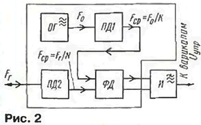
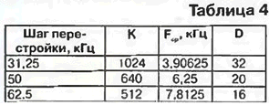
The divider PD designed so that its division ratio To is set by the processor in strict accordance with the established step adjustment on table. 4.
How does the synthesizer in the ring pulse of the PLL when the frequency lo Fг1 frequency Fг2, and Fг2>Fг1? For the inputs frequency-phase detector were the signals of the same frequency (Fcp). output the frequency of the local oscillator must satisfy the ratio Fо/K=Fг/N. Change the division factor N per unit leads to a corresponding change in the frequency F, the minimum pitch of the grid frequency of the local oscillator.
In the first moment after increasing N, the frequency of the signal at the output of the programmable divider PD will be less Fcp and frequency-phase detector will begin to produce corrective pulses which are converted by the integrator in increased voltage control (I control). This voltage is supplied to the varactors lo (a also the input circuit and a bandpass filter in each channel selector). Frequency lo will be increased to until the frequency value at both inputs. frequency-phase detector is not equal. As a result the achieved phase difference (residual detuning) will be maintained constant. Therefore, by changing the division ratio N is the restructuring of the selector on frequency. With each step value adjustment corresponds to a certain the value of the frequency comparison (tab. 4).
It is easy to see that the speed of adjustment depends on the parameters of the integrator. So, the increase of the input current of the integrator is five times causes significant the increase in the speed of adjustment. This method of management is called PUMPING (Charge Pump). However, it should be borne in mind that the speed of adjustment is limited the condition of stability, as in any system of automatic control.
In table. 4 shows also the values of the coefficient D, needed to determine the division factor N. To calculate its values using the ratio N=D(Fгн + Fпч where Fгн - frequency local oscillator signal for image, Fпч - FC image. In binary terms for the factor programming the number N has the form:
N=16384·N14+8192·N13+4096·N12+ 2048 ·N11+1024· N10+512· N9+256 · N8+ 128 · N7+64 · N6+32 · N5-4 6 · N4+8 · N3+ 4 · N2+2.N 1+N0, where N14 - N0 - bits of information, takes the value 0 or 1.
And finally, you should describe the Protocol of exchange of signals between the PLL selector and a microprocessor control system in various modes.
In RECORD mode, the Protocol consists of five bytes of eight bits each: one-byte addresses, two bytes of program divider PD and two bytes of control. In the end of each byte is the selector must send a special signal ACK (Acknowledge), confirming the correctness of the received information. In General, the exchange Protocol in this mode is presented in table. 5. It should be borne in mind that the same bits in bytes management for different models of selectors has a different designation. For example, bit P14 denote 5I, the selector KS-H-62, T14 - for KS-H-64 and CP - for the rest. Therefore, in tables such bits designated by the letter P (PORT) with serial digital number in brackets can be specified designations for specific selector. The values of the bits. noted in tables X, not used for control.
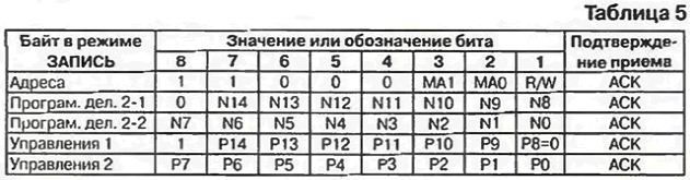
Address bits R/W (Read/Write) switches the selector switch to mode READ or WRITE. When R/W=0 is set to the RECORDING mode. For selectors without READING it - the only condition.
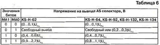
ME and MA bits select the desired address if the TV contains several selectors (for example, the second selector device for "picture in picture"). Change addresses is achieved by changing the voltage on the output AS in accordance with table. 6. When used in TV single selector MA=0 and MA=1 or output AS leave free.
Bits N14-N0 (see tab. 5) set the division ratio of programmable divider PD, as mentioned above.
Bit P14, which was already mentioned, a bit of pumping. The selector KS-H-62 P14(51) equal to 1, increases the speed of adjustment from certain frequencies in each sub-band. For the rest of the selectors with the same bit value of P14 (T14, CP) is provided by Express setup.
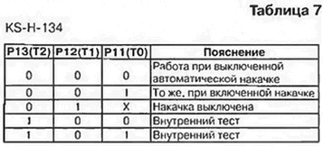
In the selector KS-H-134 bits R13 - R11 (T2 - t0) control on and off modes internal testing and automatic pump in accordance with table. 7.
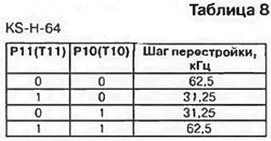
In the selector KS-H-64 bits P11(T11) and P10(T10) control programmable divider PD as shown in table. 8.
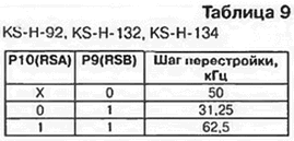
In the remaining selectors to control this divider bits used P10 (RSA) and P9 (RSB) on the table. 9, and bits P13 and P12 must be set to 0, and bit P11 - value 1. Since the selector KS-H-62 perform with a single step adjustment (62,5 kHz), then the bits for it P11, P10 and P9 is equal to 1.Bit R8 is equal to 0 for all selectors, without exception.
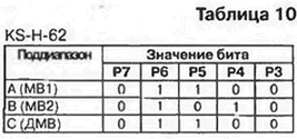
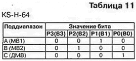
Switching sub is concentrated in the last byte of the control. And the number of bits used can be from three to five (the other bits are not apply). The selector KS-H-62 - P7 - RZ in table. 10, for KS-H-64 - RZ (OT) - P0 (B0) in the table. 11.
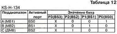
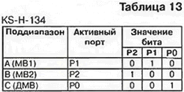
For KS-H-134 (PL. 12) KS-H-92 and KS-H-132 (PL. 13) use three low-order digit P2 (BS2) - P0 (BS0).
READ the exchange Protocol consists of baiga address and the status byte. Bit R/w in the address byte must be equal to 1. Other changes in this byte is not (see tab. 5, 14).
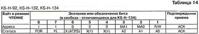
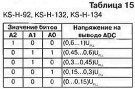
Status byte for selectors KS-H-92. KS-H-132. KS-H-134 shown in table. 14. Bit POR (Power On Reset) signals the power selector. Bit POR is 1 when the power is on. Bit FL In-lock Flag) signal about the action system PLL. When this bit FL is $ 1. the ring of PLL is closed. Bit ACPS (Automatic Charge Pump Switch flag) informs about device operation automatic the PUMP switch in the selector KS-H-134. Bit ACPS active in state 0. Bits A0-A2 outputs of patchagogo ADC (ADC). For selectors with the regime READING (see tab. 14) ADC parameters and combinations of levels A0-A2 and the same are listed in table. 15. ADC allows, for example, to control the selector three-wire bus (American standard).
A few words about the control processors. Quite a lot of them. They differ from one another by filling the internal ROM ("firmware"). For selectors KS-H-92. KS-H-132 best suited processor RSAS-30 firms PHIUPS.
Literature
Author: A. burkovsky, St. Petersburg