


")

Many switching power supplies of modern TV sets are collected at chips, in particular, the STR-S6307 and SE110N. However, their internal "stuffing" the principal schemes are often not shown, which makes it difficult to repair such sources. The article partially addresses this gap. Reader will find in it the information about the fault, the nature of their existence and also how to enable domestic transformers in various import models TVs.
IC STR-S6307 SANYO used in power supplies such TVs, how AIWA TV-1402, TV-2002, TV-2102; SONY: KV-1435, KV-1485MT, KV-2185MT, KV-RM827S, KV-14DK1, KV-21DK1, KV-RM827B; PANASONIC: TC-21L3RTE, TC-21E1RTE [1]. meanwhile, the lack of descriptions of the structure of chips STRS6307 and SE110N created a lot of difficulties in the repair of their power circuits. It was thus necessary to thoroughly examine and reveal the construction of these chips. This problem was solved by comparing circuits STRS6307, STR-S5941 and STR-10006 [2]. To determine the structure SE110N was taken as a basis chip SE014N [3]. Continuity STRS6307 and SE110N, electric range tests allowed to determine the values of its components.
To verify the correctness of disclosure patterns and to investigate the possibility of replacing damaged circuits STR-S6307, SE110N their discrete equivalents, and the possibility of replacing failed transformers 36-A (АIWА), SRT (SONY) ET834K407A (PANASONIC) domestic TPI-8-1 and TPI-5 was assembled source power on domestic parts and transformer TPI-8-1. Your device securely working under the load of 50…80 W as in the Assembly of hinged parts, and using ICS STR-S6307 and SE110N.
In an experimental power source faults were introduced. Description of how the source reacts to them, is given at the end of the article. Schematic diagram power AIWA TV-TV1402/2002/2102 shown in Fig. 1 (chain network and the secondary rectifiers are simplified). Transistor KTA (VT1 chip IC801) can be replaced by CTA, BU508A, BU2508A, 2SD1710, transistor 2SA817A (Q801) - CTB, transistor 2SC3852 (Q822) - CTA, diodes and EG1Z EU1Z (D803-D805) - CDD - KD243ZH. Zener diode D807 can serve DD.
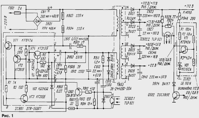
The source operates as follows. A voltage of about 300 V with capacitor C after turning the TV on via the trigger circuit of R803, R804, pin 3 of the chip IC801 is supplied to the base of switching transistor VT1 of this chip. Transistor starts to open. Through it, the coil magnetization 7-5 transformer T and the resistor R805 (sensor current) flows linearly rising current. In the winding positive feedback (PIC) 1-2 transformer electromotive force occurs mutual flows and increasing the base current of the transistor VT1 with output 1 the transformer via the output terminal 5 of chip IC801, the divider R5R4, emitter transitions of transistors VT4 VT1 and, IC801 pin 2 to pin 2 of the transformer.
After reaching a certain value, the voltage from the resistor R805, is applied through pins 2 and 7 of the chip IC801 and the resistor R1 to the emitter junction of transistor VT3, opens it. The winding current PIC is closed through the divider R5R4, emitter transitions of transistors VT4 and VT2, VT3 transistor and resistors R3, R805. Transistor VT2 open, sunterra emitter junction of the transistor VT1 and closing it. Voltage to change polarity windings. Their positive pulses recharges the capacitor filters the secondary rectifiers. Then everything repeats.
This happens a few cycles of opening of the key transistor VT1 through the chain run. After that, the secondary rectifiers capacitors are charged almost to nominal stress and fail to load the transformer. As a result source goes into self-oscillation mode.
In self-oscillation mode when the switching transistor VT1 is closed, the winding 1-2 the transformer has a voltage of the PIC (plus at pin 2). The current of this winding charged capacitors: C - through pin 2 IC IC801, diode VD1, conclusion 3 IC801 and resistor R810; C814 - through IC801 pin 2, diode VD2, pin 4 of IC801 and diode D803; S - through resistor R807, IC801 pin 9, diode VD3 and the IC801 pin 5.
When charging currents of the capacitors of the secondary rectifiers is reduced to zero, the voltage across winding 1-2 of transformer also becomes zero. The capacitor voltage C through resistor R810, winding 1-2 of transformer and conclusions 2,3 IC801 affects the emitter junction of transistor VT1 and reveals it. Increasing the current of the winding 7-5 transformer causes in his the winding 1-2 voltage on the plus terminal 1. Via terminals 5 and 2 of IC801 and the divisor R5R4 it is applied to the emitter transitions of transistors VT4 VT1 and.
On elements VT4, R4, R5, VD2, C814, R808, D803 assembled node maintain a current the base of the transistor VT1. Current winding 1-2 of transformer, passing through the emitter transitions of transistors VT4, VT1, opens them. When the capacitor C discharges through them, creating the base current of the transistor VT1.
Transistor VT1 is switched off by the transistor VT2. He, in turn, is controlled site off-current on the elements VT3, R805, R1, R3, and site stabilization the output voltages on the transistor Q801, optocouplers IC802, chip IC821, diodes D804, D805 and the Zener diode D807.
The Executive part of site stabilization simplistically depicted in Fig. 2. The collector voltage on the transistor Q801 is the sum of the voltages on the winding 1-2 of transformer and condenser C, charged through the diode VD3 and resistor R807 when closed, the transistor VT1. Elements R811 and are S the lower arm of the voltage divider bias the base of transistor Q801. Upper shoulder formed by resistor R814 and the phototransistor of the optocoupler IC802. Through the led OPTRON IC802 (see Fig. 1) flows a current output node of the comparison transistor VT1 chip IC821. The phototransistor of the optocoupler (see Fig. 2) reduce your the resistance by increasing the output voltage V. 112 results In changed the emitter current of the transistor Q801, representing a portion of the base current transistor VT2 (see Fig. 1). Transistor VT2 changes the moment of its opening and bypass key-emitter junction of the transistor VT1.
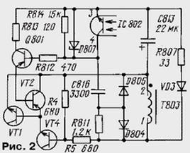
A protective Zener diode D807 is designed to increase the current of the transistor Q801 when a sharp increase in the amplitude of the pulses in the winding 1-2 of transformer, for example, due to breakage of loads. Diode D805 together with the resistor R811, R4, R5 limits the amplitude of the pulses in the winding 1-2. Diode D804 with a resistor R811 is to recharge capacitor C during the closed state of the transistor VT1 through the collector junction of transistor VT2, the emitter junction of transistor Q801 and resistor R812.
In the event of failure of transformer T (AIWA), T601 (SONY), when you can't to reach the damaged winding, the power source can be set pulse transformer RT-8-1. The scheme of connection in the TV AIWA presented on Fig. 3. The voltage is +8.6 V to power source STANDBY +5 V and node alarm reset on-chip IC822 (ST3050R) is provided additional elements VD1, C1, C2, DA1.
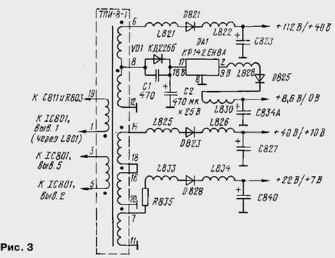
The simplest can be called a connection diagram of the transformer TPI-8-1 to a SONY TV. It uses only four winding transformer: the magnetizing winding 19-1, winding the PIC 3-5, winding 6-12 source 115 and In winding 16-20 source 15 V.
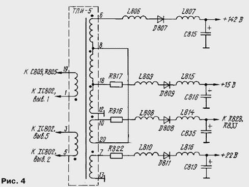
To replace the transformer T PANASONIC TV fits the TPI-5. Scheme connections depicted in Fig. 4.
Faults occurring in the device, can be divided into two groups: damage inside the chip IC801 and IC821 and defects of hinged elements.
The cliffs in the transistors VT2 and VT3 chip IC801 inevitably lead to the breakdown of a transistor VT1 and the blown mains fuse.
At the precipice of the resistors R803, R804 output voltage is zero. The same occurs and when the circuit R810, C815, winding 1-2 of transformer T.
In case of breakage or loss of capacity of the capacitor C output voltage source 112 is reduced to 97 V. The same occurs and breakage of the resistor R808. The breakage of the diode D803 causes a decrease in voltage source 92, and capacitor S to 32 V.
On the contrary, the breakage or loss of capacity of the capacitor C increases the voltage source to 160 In, is heard quite strong whistle.
In case of breakdown of the transistor Q801 voltage source 112 is reduced to 20 and In audible monotone.
At the breakdown of the emitter of the transistor Q801, optocouplers or IC802 transistor VT1 chip IC821 the source voltage also increases to 160 and heard a strong whistle.
Prolonged work with a dangling loop of automatic control, when the output voltage is 160 V, causes breakdown of the transistor VT1 in the chip IC801 and the output transistor horizontal.
Literature
Author: I. Molchanov, Moscow