


")

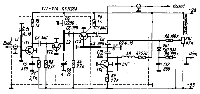
RF amplifier Converter - gascogny, transistors VT1, VT2. His load is a circuit L2C5. Through the capacitor C6, the signal passes to the emitter of the transistor VT3 of the frequency Converter. Appropriate connection of the cascades to the line 1.2 are consistent output (RF amplifier) and the input (Converter) resistance in selected q-factor of the circuit.
The voltage of the local oscillator is removed to the base of transistor VT3 Converter with part of the line L3. It forms with the capacitor C9, the local oscillator circuit, performed on the transistor VT4 scheme of capacitive treatacne. The ratio of the turning on of the transistor in the circuit is determined by the ratio of the capacitance of the capacitor C11 and capacity-emitter junction of a solar cell. The change in capacitance diode VDI, connected to the circuit through capacitors C8 and 12, it is possible to smoothly adjust the local oscillator within the same channel. For this purpose, the diode filed closing its voltage, which regulate a variable resistor R10. The resistor R7 prevents self-oscillations throttle.
Increased sensitivity of the Converter compared to similar devices achieved by choosing the optimal mode of operation of the transistor VT1 to noise ratio and the use of stable bipolar source of supply voltage. This food has helped to create a common base of the transistors of the Converter constant current, i.e., to connect the base directly with the common wire and without dividers in their circuits and bypass capacitors for alternating current. It helped get rid of the last characteristic high-frequency noise flicker capacity, to reduce the number of parts and, consequently, the resulting parasitic capacitance and inductance. The lack of a blocking capacitor in the base circuit of the transistor VT4 lo allowed to obtain a higher spectral purity of the generated oscillations [1]. Furthermore, the use of the bipolar power source completely solved the problem of thermal stabilization of cascades.
The noise of the transistor VT1 depend on the mode of DC, and the coordination of the input of RF amplifier. Measurements have shown [2] that the noise factor of the cascade bipolar transistor practically does not depend on voltage collector - emitter and increases only at small values (less than 3). The same dependence from the collector current for most modern microwave transistors has a weakly pronounced minimum at values of 1 to 5 mA. The most significant factor increasing the sensitivity of the Converter is the provision of a so-called optimum mode mismatch at the input of RF amplifier, wherein the noise figure of the cascade is reduced to a minimum value. The calculation of this mode is simple, but assumes the presence of regime-frequency characteristic of the Y-parameters of the transistor used, which are not always available to radio Amateurs. Therefore, if instead of those on the scheme you intend to use other transistors, we can proceed as follows. As the active component of the input admittance of the transistor depends on the collector current, the maximum sensitivity of the Converter can be achieved by changing it in the range of 1…10 mA. Although the collector current is unlikely to correspond to the minimum self-noise of the transistor, the loss in noise figure after careful tuning, even in the worst case will not exceed 0.5 dB compared to the minimum achievable [3].
Details. In the Converter used fixed resistors MLT (R1-R3 is group A, i.e., the normalized voltage noise not more than 1 µv/V). Variable resistor R10 is any resistance 47…100 kOhm. Trimmer capacitors C1, C5, C9 - PDA-MP, straight C4 - KTP or any suitable dimensions 180 4700… pF, the rest, except SI,- km, FC 100…620 pF.
Note that the radial and axial play of the rotor in the trimmer capacitors is invalid. The capacitor C11 (1PF) - a piece of 75 Ohm cable with ftoroplastovaja insulation (heat input capacity of 0.55…to 0.67 pF/cm) with a length of about 20 mm (specify when establishing, starting with 35mm). The inductor L4 is wound in bulk on a paper frame with a diameter of 3 mm and contains 100 turns of wire sew-2 0,1 (winding length - 5 mm).
Instead of the diode CDA you can apply KDA. KDA or KD521, KD522 with any letter index, instead of transistors CTA - GTZ, CTA, CTA, any of the series CT, GT, GT, CT and CTA, CTA, CTA (named in order to improve the parameters of the Converter). When using a transistor structure n-p-n it is necessary to change the polarity of diode VD1 and power sources.
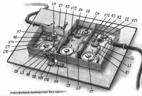
Fig.2
The design of the Converter shown in Fig.2. Installation - space-printed, using the Board, the drawing, which presents Fig.3. It is made of two-sided foil fiberglass with a thickness of 1.5 mm. as in the UHF range the penetration depth of high frequency currents in the copper printed conductors does not exceed a few micrometers, to reduce high-frequency losses in the metal and improve the quality of the oscillatory circuits of the roughness of the surface of the Board from the mounting should be as small as possible. To do this, it is polished to a mirror finish grinding microporosity, GOI paste or toothpaste and coated with a thin layer of any nitrocellulose lacquer dissolved with acetone in the ratio 1:2. This treatment will prevent oxidation of the surface layer of copper and permanently retain its high conductivity. When mounting the foil in the soldering joints of the parts clear varnish sharp end of a knife. Since the conductivity of the solder is approximately an order of magnitude worse than the conductivity of copper, tinned large areas of foil not recommended, the amount of solder in the soldering should be as low as possible.
The conclusions of elements should be as short as possible, the separation and their bypass capacitors otpaivaete quite, pre-clearing the soldering points from the paint. The transistors are rigidly inserted into designated holes (when using other transistors, these openings may never be needed). To reduce the impact used the screwdriver on the frequency of the tuning circuits of the findings of the rotors trimmer capacitors C1, C5, C9 soldered to the PCB (GND), petals-conclusions stators bite. Compounds of the conclusions of parts (two, three or four), shown in the drawing without soldering points are located above the Board. Dots indicate locations of soldering to the foil on the appropriate side of the Board.
Lines L1-L3 are stretches of bare polished copper wire of diameter 1 mm and length 22 (L1, L2) and 24 (L3) mm. One end of each line wire soldered to the output of the stator of the trimmer, the other to GND, creasing along the radius of 7 mm (LI, L3), or to the conclusion of passing capacitor C4 (L2). The segments come on Board at a height of 5 mm for the 21st - 35th channels and 3 mm for the 36th - 39th channels. The distance to pripiski elements (counting from the ends connected to GND directly or through a capacitor C4) L1 - 4.3 and 5.5 mm, L2 = 3.5 and 12 mm at L3 - 4 mm.
For shielding the stages of the Converter soldered to the Board walls and partitions with a height of 12 mm made of copper or brass with a thickness of 0.3…0.5 mm with cut-outs and holes under the findings of the elements. The output circuit of the Converter screening is optional. After establishing the installation close the top cover of the same material with holes for access to the rotors of the condensers C1, C5, C9. For the purpose of increasing the mechanical strength of the antenna and the output cable is fixed on the PCB with a wire staples.
The establishment of the Converter start with checking the supply current, which should be equal to about 10 mA. To power at this stage it is desirable to use galvanic cells, thus avoiding the possible impact of the surge and interference from the stabilizer. Then make sure in the work of the local oscillator, which is connected to the output of the Converter to the input of the TV that is included on a free channel. Work of the local oscillator power to the Converter leads to an increase in audible noise, and the rotation of the rotor of the capacitor C9 to the change of their intensity and the flashes on the TV screen. If not, as the capacitor C11 includes a segment of coaxial cable has a length of 35 mm. achieve the Desired result, gradually shortening it with a sharp knife (if the cable diameter less than 3 mm, it is necessary to ensure that after cutting the braid was not connected to the Central conductor). In the case of failure described procedure is repeated with increased emitter current of the transistor VT4, which reduce the resistance of the resistor R6 to 1.5 ohms.
After achieving a stable operation of the oscillator, adjust it to the desired frequency. To do this, connect the antenna cable to the left (the scheme), the electrode of the capacitor C6, pre-hotpaw it from the line L2. Rotating the rotor of the capacitor C9, achieve the appearance of at least a faint image on the TV screen when you receive on the selected channel MB. Restoring the connection of the capacitor C6 with line L2, connect the antenna cable through capacitor 10…30 pF to the emitter of the transistor VT2 and, rotating the rotor of the capacitor C5, tune the RF amplifier circuit according to the best image on the screen. If the resonance phenomena are absent, i.e. the position of the rotor of the capacitor C5 does not affect the image quality, adjust the inductance of the line L2 by changing the height of its location on the Board. Then apply a signal to the input of the Converter and thus tune the input circuit L1C1.
Further, instead of the resistor R2 include serially connected to a constant resistor of 820 Ohms and a variable resistance of 10 ohms. Changing the last emitter current of the transistor VT1 and adjusting the input circuit to achieve the maximum sensitivity of the Converter for the highest image quality. By measuring the impedance of the resistors in the emitter circuit, replace them with a single resistor with the closest value.
On the propagation of UHF significantly influenced by meteorological conditions. Therefore, in-countryside, located in a zone of uncertain reception mode transistor VT1 for the best sensitivity, it is desirable to pick up at a settled weather for a few hours before or after sunset.
In conclusion, close the Converter cover, soldered it around the perimeter to the walls of the screen and through the holes in it eventually adapts to the contours of L1C1 and L2C5. It should be remembered that the tuning of the input circuit is sometimes necessary when changing the length of the antenna feeder, the location of the antenna or replace it with another one.
Literature
Author: M. Zaitsev, Elektrostal, Moscow region; Publication: N. Bolshakov, rf.atnn.ru