


")

In this article I would like to focus audiophile on the effect that many recently called transistor, some long are fighting it in RF and microwave technology, some in the combating release interconnect and speaker cables costing up to thousands of U.S. dollars, someone is trying to present this the effect is nothing more than just… hallucinations audiophiles! Below I will tell you how in a few evenings at home from scrap materials to manufacture superior (i.e. absolutely neutral in a wide range frequency) audio cable, not inferior in quality to the best world samples. But before that everything was in its place, I will say the following: all audio and high-frequency radio equipment designed incorrectly!
Next on the text provides your likely questions.
We are without you have long suspected. What same thing here?
It is known that the passage of alternating current to the conducting layer conductor or semiconductor so-called surface effect (skin effect). Most of the moving electric charges due to electromagnetic induction is near the surface the conductive layer. Negative effect skin effect is manifested in that large Central portion of the conductive layer is not involved in the transfer of electric charges, which causes increased resistance conductor of electric current. In addition, the skin effect in metal the wires and the plates of the capacitors leads to slow redistribution of mobile electrons from the centre to the surface, due to what you experience unwanted effects of orientation and reseating the cables, but in the capacitors increases the memory effect. Negative action skin effect on cables and wires is compounded by the fact that the chemical compounds of the metal conductive layer with the oxygen and nitrogen of the air, formed on the surface of the wire due to corrosion, have dielectric and semiconductor properties, which, in turn, promotes the growth of losses and distortion. The degree of manifestation skin effect depends on the frequency of the current. More precisely, from the instantaneous frequency of the current.
With increasing frequency the thickness of the surface layer through which the current passes, reduced. In the case of a broadband signal, where the instantaneous frequency with difficult to describe, the skin effect causes a mess in the placement moving electrons in a cross section of the conductor. The consequence of this are nonlinear and intermodulation frequency phase distortion electric broadband signal passing through the conduit or the semiconductor. In consumer and professional audio equipment skin effect connecting interconnect and speaker wires lead to noticeable on distortions of signals, deteriorating the quality of sound reproduction.
In the radio receiving apparatus of the effects of skin effect (for example, in the cable, connecting the antenna with the input of the receiver) created intermodulation distortion broadband signal lie in the reduction of selectivity, reducing the signal-to-noise and decrease sensitivity. It is known that the passage of the alternating current through the conductor primary (utility) of an electromagnetic wave extends along the conductor in a straight line between points with different the potentials. Because of skin effect in addition to useful wave occurs unwanted spurious electromagnetic waves directed from the Central axis of the conductive element to the surface, perpendicular to the direction of wholesome wave, causing phase distortion passing signal.
In digital switching devices, for example, computers, due to the skin effect in copper conductors and printed circuit boards connectors distorted form of short pulses, which leads to breakdowns synchronization failures in reception of pulses. This is the main obstacle increasing the clock frequency in motherboards and connectors on computers. On high and ultra high frequencies the skin effect drastically reduces the quality factor of the jet elements like capacitors and inductors.
As a consequence, on frequencies above 1 GHz, the skin effect is the main factor limiting miniaturization of electronic products, such as chips. It is the skin effect is responsible for the so-called effect transistor sounding. In the transistors of the cross-sectional area of the crystal is much smaller the cross-sectional area of the electron cloud, as areas of the cathode and the anode in the tube. the form, contact pads on the surface of the crystal transistor connected thin wires (this knows anyone who ever seen the transistor without housing), in which the skin effect live very freely.
What can be done to combat this the phenomenon?
I can recommend a cheap and effective way of neutralizing skin effect. It is based on the fact that the material is overwhelming most conductors (copper, silver, aluminum, brass) and semiconductor (silicon, germanium) elements has a record of the relative magnetic permeability m from 0,9999 to 1,0001, i.e. about units.
The surface of the conductive element 1 is coated paramagnetic the shell 2 (see Fig.), moreover, the shell is not necessarily tightly snugly, there may be some small gap. The shell is in the form of one or more layers of solid paramagnetic m is greater than 1 a dielectric material (magnetodielectric), which macro-level indicator of the relative magnetic permeability m, several times exceeding the permeability conductive element, low electrical conductivity and low loss for remagnetization (loop hysteresis). In Fig. for clarity, shows the two layer sheath: a layer 3 and layer 4. The shell needs to be fixed immovably relative to a conductive element on its surface; in the case of the gap width not should exceed half the wavelength of the alternating current in the conductive element.
So what gives?
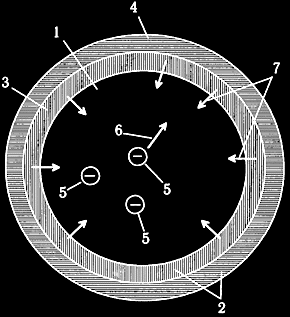
Flowing in the conductive element 1 is perpendicular to the plane of the gure the alternating current creates a conductive layer inside the undesirable element 1 transverse electromagnetic field of skin effect. The lines of force 6 this field act on elementary moving charges within 5 conductive element 1 and is directed from the center of the conductive layer to the surface. At the same time, the main (good) AC current signal flowing through the conductive member 1, creates a layer 3 and layer 4 paramagnetic shell 2 opposing magnetic field force lines 7 which are directed from the surface of the conductive member 1 to its center and is also affected basic moving charges inside the conductor 5 1. The intensity and that, and the other fields increases with the current and with the growth frequency. Eakin results in compensation of the parasitic action transverse field and a uniform distribution of electric current around the cross section of the conductive layer.
For most low-power conductive elements to achieve a positive effect paramagnetic shell may be made of a material with an index of the relative magnetic permeability of from 1.5 to 20 thickness of several tens of microns or more. For power conductor elements, at small the dimensions of the conductor, as well as for low-frequency devices, the casing may to be of similar thickness when the value of m from 1.5 to 50, if the shell material has index greater than 50 m, and the length of the conductive element significant (a few meters), along with the parasitic transverse wave useful wave will also be suppressed to increase their own cable inductance and losses in the shell itself, and passing the signal get the phase shifts.
For clarity, the principle on which this is based the way to deal with skin effect, can be compared with magnetic or electromagnetic focusing of the electron beam in cathode-ray the tube, for example, a television picture tube. In the kinescope electron flow moving with acceleration in a vacuum under high anode voltage from the cathode to the anode (the screen). Moreover, due to vzaimoottalkivanie actions falling on the screen, the electron beam forms a vague blur. Therefore, a forced beamforming, what are coil, creating an annular electromagnetic field around the electronic of the beam. aeacus is achieved focus and consideration.
I propose to use for paramagnetic shell mixture of dielectric (for example lacquer, resin or polyvinyl chloride) with conductive powder a soft magnetic material (for example, powdered permalloy or occifer). The volume ratio of the dielectric and magnetic material selected so that to the electrical conductivity of the mixture was insignificant compared to electrical conductivity of the conductive element. I also propose to use a mixture of a dielectric polymer with powders of substances such as dioxide chromium CrO2, gamma-iron oxide Fe2O3, cobalt-γ-iron oxide CoFe2O3.
These magnetic materials have a relative magnetic permeability from 1.5 to 2.0 and have a small time of reversal. They are produced industry for audio and video recordings, their cost is small, although in a strong magnetic field, these materials have a relatively high coercive force, in most electronic elements of power flowing through them current is not high enough for the existence of magnetic properties of these materials. Therefore, in this case, the loss on hysteresis in the shell are small, which allows to achieve a positive effect. In the manufacture of flexible, high quality (audiophile, as now fashionable to say) unshielded interconnect or acoustic cable (the author used a conventional chromium-dioxide tape width of 12.7 mm based on the pet). wenta is wound with an overlap of 6 to 10 layers the main metal (copper or silver) conductor. In the result of this operation is greatly reduced nonlinear distortion introduced cable, and the upper frequency bandwidth of the cable increases from 30 MHz to 120 - 250 MHz and above, depending on the thickness of the wire. The cable is in the form of three woven braid conductors (such as as does the firm Kimber Kable).
In addition to the manufacture of cables described method of dealing with skin effect can be applied at industrial level in relation to the conductive items of all shapes and kinds, made of conductors, superconductors and semiconductors with an indicator of the relative magnetic permeability about units intended for passing current and current-control a wide range of power and frequency. zayavlennyj method can be applied, for example, in the manufacture of communication cables, mounting and connection of wires, transistors, diodes, integrated circuits, contact devices, connectors, resistors, electrical capacitors and high frequency inductors.
And what do we get as a result of applying your suggested method?
Get pleasure from listening to music.
Author: Sergey Podolyak, Vinnitsa, Class a; Publication: www.audio.ru/class_a/home.php, www.cxem.net