


")

It is sometimes necessary to alternate switching multiple loads with electronic keys instead of a mechanical switch. Literature search led to an interesting technical solution, published in Radio No. 12 of 1989.
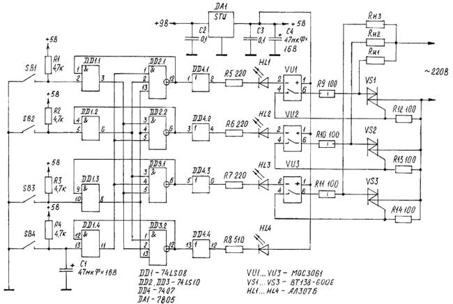
Electronic switch loads works as follows. At power-up, capacitor C1 begins to charge through resistor R4. Low voltage at the capacitor C1 in the first time sets at the exit of the element DD1.4 log. "0". The outputs of the elements DD2.1, DD2.2, DD3.1 set log. "1", the outputs DD1.1, DD1.2, DD1.3 also set log. "1", the output element DD3.2-log. "0". Led should be illuminated HL4, indicating the device is ready, but none of the load is not included. To enable, for example, the load Rн1, click button SB 1. Thus at the exit of the element DD1.1 set log. "0", the output element DD3.2 - log. "1", and HL4 led turns off; at the exit of the element DD1.4 set log. "1" because C1 is already charged; at the output of the element DD2.1 set log. "0", the output element DD4.1 - log. "0".
HL1 led is lit and indicates the inclusion of the load. Optocoupler key VU1 opens the triac VS1, and that, in turn, switches the load Rн1. Elements of the chip D4 are used as repeaters with high load capacity. When you press, for example, the button SB3, first turn off the load Rн1, as at the exit of the element DD1.3 set log. "0", the output of the element DD2.1 - log. "1" and the load Rн1 is disabled. At the output of the element DD3.1 set log. "0", the output element DD4.3 - also log. "0", the HL3 led lights up and turns on the load n R 3.
Circuit a circuit design eliminates even the inclusion of two short loads. To disable any of the loads you can press button SB4. Optionally, you can include a fourth load, adding to the chain of HL4 led chain of optolyth and triac, similarly to the above circuits. Power switched load is determined only by the maximum current applied to the triac. Thus, pressing the low button SB, you can switch loads from hundreds of watts to several kilowatts.
A modified scheme is shown in the figure.
Details
To power the circuit uses a transformer with a diode bridge rectifier and filter, with an output voltage of 9 V. the Voltage supply to the chip stabilizes chip DA1 type 7805. Indicated on the diagram of the chip can be replaced by domestic counterparts: 74LS08 - CLI, 74LS10-CLA, 7407 - CLI, 7805 - CREA. Button SB1-SB4 type SWT2-7 can be replaced by any domestic.
According to the magazine, glad I oamator.
Publication: www.cxem.net