


")

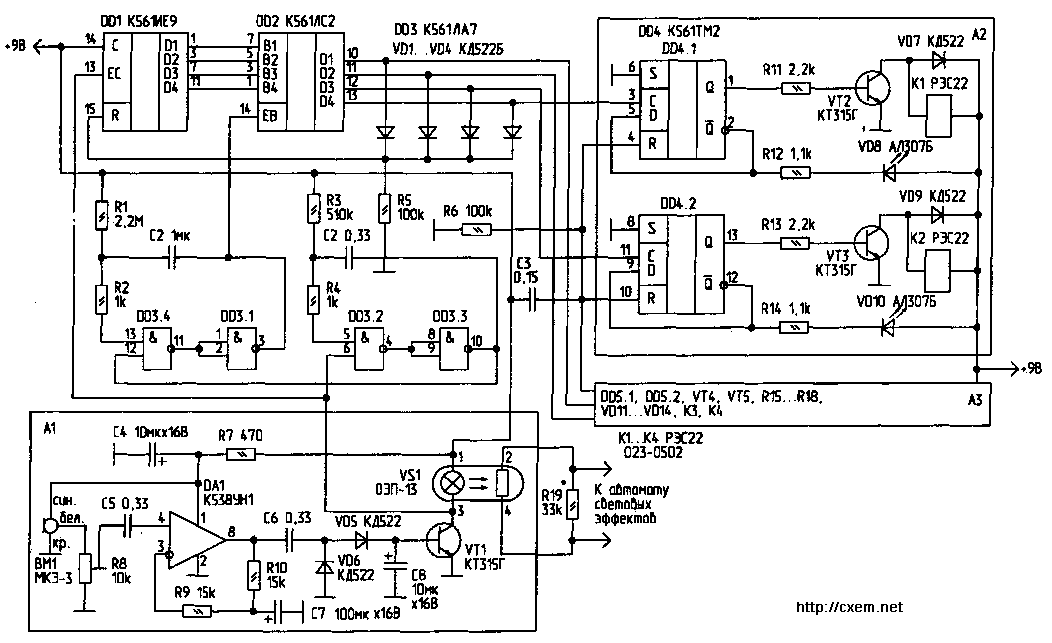
The proposed switch, schematic diagram of which is shown in the figure, in addition to its primary function to enable/disable one of the four loads (depending on the number of claps) and controls all automatic lighting effects. In most machines the lighting effects used by the master oscillator, the frequency of which is regulated by a variable resistor. So either the speed of switching of lamps or lights does not match the tempo of the music, or have each melody to reconfigure the generator manually. This acoustic switch allows you to switch garlands in accordance with the tempo of the music. In the absence of music or in the pauses garlands switch with a minimum frequency that is set by selection of resistor R19.
I used this acoustic switch paired with the automatic lighting effects on EPROM CRC [1], in one case, using relay 4-channel to enable (+5V - powered circuits, -220 In the power of the garlands). The sensitivity of the switch is adjustable trimming resistor R8, so that he reacted to the music, but I was changing channels switching loads. Practice shows that in addition to involved the 4th channel, just use the 2nd and 3rd channels, and from using the 1st channel should refrain, as in sharp bursts of music may be triggered.
Consider a job switch. With microphone VM via trimpot resistor R8, the signal is input to the amplifier-limiter on the chip CAN. After amplification, the signal is detected by diodes VD5, VD6 and is supplied to the base of transistor VT1. In its collector load resistor-tion optocoupler EIA-13, which drives a generator of automatic lighting effects. Thus, the burst noise spectrum of melody opens the transistor VT1, and the output resistance of the optocoupler (pins 2 and 4) is reduced, which increases the switching speed of garlands. The VT1 transistor opens fully (the degree of opening is governed by the resistor R8, so that didn't work, the switch loads).
(click to enlarge)
With a fairly strong cotton VT1 opens fully, the low level runs of the first standby multivibrator elements DD3.2 and DD3.3, which operates as a delay time t, defined by the elements R3 and C2. When specified on the diagram the values of R3 and C2 t=0.3 s. the Delay is necessary to prevent false positives decimal counter DD1 (account more than one pulse). Low collector VT1 is simultaneously input of the counter DD1. The second multivibrator lengthens pulse input when R=2.2 Mω and C1=1 µf approximately 4 s. the time during which goes by the number of claps counter DD1 and there is a ban on information read from the chip DD2.
For example, you made three cotton. Counter DD1 issued at the output of D3 is positive. At the end of the 4 with the control input of the chip DD2 established a high level that allows the transmission of a logical "1" from input OT output D3. This trigger level DD4.2 is shifted to the opposite state. The key VT3 controls relay K2, which switches the load N2. At the same time the high level output from the D3 of chip DD2 through the diode VD3 resets counter DD1. Led VD10 signals the introduction of an appropriate load. Chain R6, NW sets all flip-flops to the zero state while the device is on.
Block A1 can be used separately to control only the automatic lighting effects. If this is not necessary, instead of the optocoupler VS1 to the collector VT1 turns on a DC resistor with a resistance of 10 ohms.
Publication: www.cxem.net