


")

The generator of a smooth range (GPA) is one of the most critical components of an Amateur transmitter, receiver or transceiver. Problem high GPA is particularly acute in modern equipment, where increasingly used high-frequency quartz filters. In this case, the desired GPA, working at relatively high frequencies (tens of megahertz). Get good options from the GPA. made by traditional schemes, these frequencies is difficult.
Driver frequency can be performed by the block diagram depicted in Fig.1. Here G1-- reference generator D1 is a divisor of frequency (U1 - phase discriminator, Z1 is a low pass filter, G2 generator, voltage controlled, D2 - frequency divider with a variable division ratio. This device is an active digital synthesizer frequency divider with a variable division ratio. This synthesizer allows to obtain at the output, depending on the selected division ratios D1 and D2. a grid of frequencies with a step to several kilohertz. So, if you have a reference generator GI operates at a frequency of 5 MHz, the divisor D1 reduces the frequency to 500 times, by changing the division ratio D2 from 2000 to 2100, it is possible to obtain a grid of frequencies at the output of G2 from 20 to 21 MHz in 10 kHz.
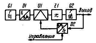
Fig.1
If the reference oscillator to take the stability of the GPA, it is possible by modifying the range of G2 and the division ratio of D2 to obtain the necessary for heterodyne transceiver frequency. The dividers work is quite simple, as the required division ratio is generally small.
This principle was used in the local oscillator of the transceiver presented at the 30th national radio exhibition. Schematic diagram of driver frequency is shown in Fig. 2.
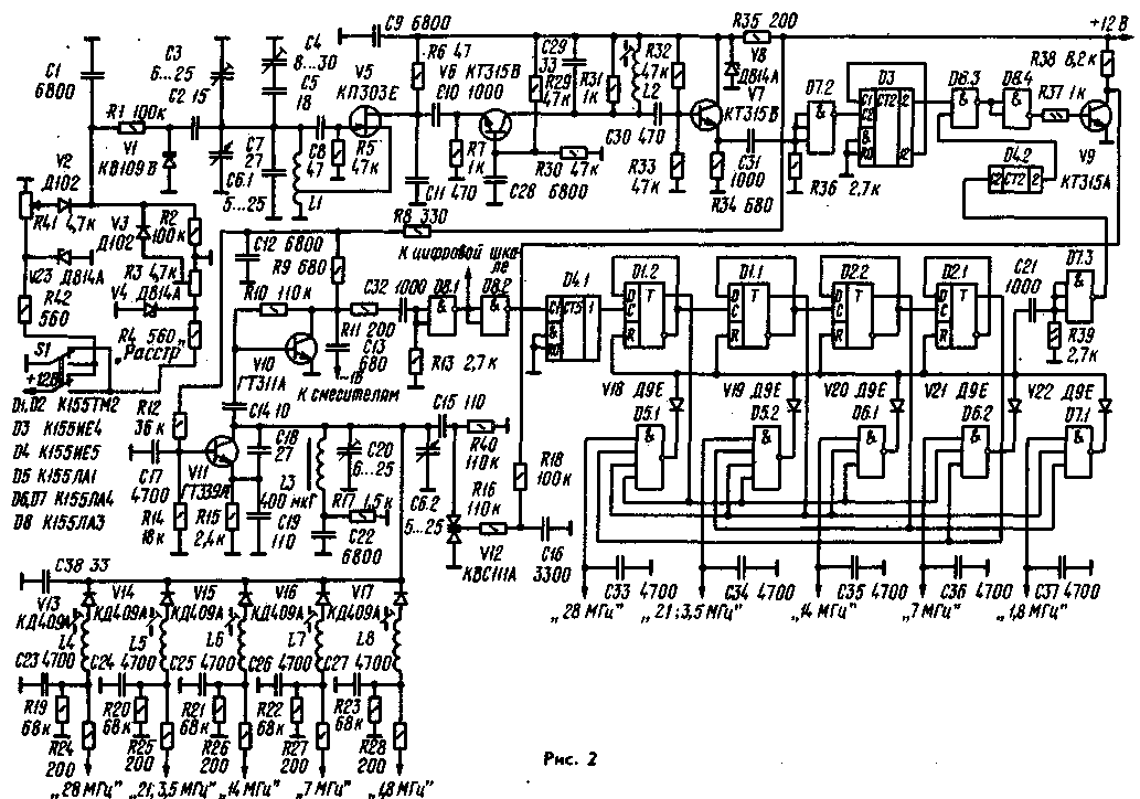
(click to enlarge)
When first enabled, the drive is $ 8750 kHz, and the signal formation of the upper side band of the required heterodyne frequency 19,25…in 20.25 MHz for the range of 28 MHz; 12.25 12.75… - ranges 21 and 3.5 MHz; 5.25 In… ...5.6 MHz to 14 MHz band; 15.75 16.25…and 10.5…11 MHz respectively for bands 7 and 1.8 MHz.
GPA that overlaps the frequency range of 5.25…5.6 MHz assembled on the transistor V5. The stability of the GPA provides a rigid structure, the use of contour coil L1 wound Venetico on a ceramic frame, the use of temperature compensation (capacitor C5 has a negative TKE); small link generator with cascades and subsequent stabilization of the supply voltage. The frequency of the GPA rebuild section C6.1 triple block capacitors. For detuning at admission (or transfer) to the varicap V1 is energized or charged by the resistor R3 when configuring the unit, or variable resistor R41 adjusting.
Transistor V6 is assembled buffer amp, loaded on a broadband circuit L2C29R31. and the transistor V7 - emitter follower. With the repeater signal is supplied to a pulse shaper based on item D7.2, and further the frequency divider (IC D3).
A controllable oscillator is performed on the transistor V11. The range is chosen, connecting to the circuit of the generator through the diodes V13-V17 (via resistors R24-R28 are served voltage of 12 V, for opening them) one of the spools L4-L8.
With a broadband amplifier transistor V10 signal generated by a controllable oscillator, is fed to the mixer and pulse shaper (element D8.1) and further to the digital scale and the frequency divider on the chip D4. The experiments showed that the driver on the element "2I-NOT" series K155 in combination with a divider CIE is stable at frequencies up to 35…40 MHz.
The divider with variable division factor is assembled on a D-trigger circuits D1 and D2. To get the desired division ratio, uses elements of D5.1, D5.2, D6.1, D6.2, D7.1, included in the feedback loop divider. So, to obtain a division ratio of 11 (range 10 m) is an element D5.1. One of its managing inputs. With the advent of the divider of each of the eleventh pulse on three inputs D5.1 logical 1 appears. If PA fourth input D5.1 is a logical 1 (on a 10 m range), the differential output D5.1 will set the divider to the zero state.
The reset pulses are simultaneously output pulses of the divider with variable division factor, which through the element D7.3 are fed to the divider D4.2 (used first trigger divider-by-eight chip CIE). D4.2 rectangular pulses on the phase discriminator performs the function element "2I-NOT" D8.3. To the second input element of the signal comes from the divisor D3 of the frequency of the GPA.
Selection of division ratio due to the bandwidth of the GPA and the required frequency of the strobe on the phase discriminator. The latter, in turn, tend to choose like this. to combine on the scale start ranges, as well as, to simplify the divider with a variable division ratio. These requirements are contradictory. When the intermediate frequency transceiver 8750 kHz and the initial frequency of the GPA 5250 kHz the initial frequency of the controlled oscillator and GPA ranges 10, 15, 20, 40, 80 and 160 m respectively equal to: 19,25/5,25 -11/3; 12,25/5,25 = =7/3; 5,25/5,25=3/3; 15,75/5,25=9/3; 12,25/5,25=7/3; 10,5/5,25=6/3. This shows that the division ratio of the divider with variable division factor (the number in the numerator) must be equal to 11, 7, 3, 9, 7 and 6, and the division ratio of the divider D3 (the number in the denominator is 3. Given that the front of the divider with variable division factor and after him are divisors of two, improving the conditions of the work and of the phase discriminator, the frequency divider is necessary to increase the conversion rate by 4 times.
It should be noted that in the above case, you can choose other dividing ratio of a divider.
At the coincidence frequency signals coming from D3 and D4.2, the output element D8.3 are rectangular pulses of the same frequency, but the duty cycle of which depends on the phase relationship of the input signals, and as a result of the correlation of the phases (including dividers) GPA and operated generator. From the same depends on DC voltage component of the output signal. After the inverter (item D8.4) and the amplifier transistor V9, the signal is supplied to a low pass filter R18C16, whose task is to suppress the impulses coming from the discriminator, and skip this constant component and a limited band of lower frequencies.
The signal from the filter is fed to the varicap V12, part customizados circuit of the controlled oscillator. To facilitate the seizure frequency in the ring phase AHR, without entering the device auto scan, circuit of the controlled oscillator connected to the free section of the block of variable capacitors. Here we use the fact that the coefficient of adjustment on all ranges the same.
If the low pass filter to apply elements with the values indicated in the diagram, side signals, which arise due to the phase modulation frequency of the controlled oscillator pulses have passed through the filter, the output signal of the local oscillator are suppressed will not be less than 75 DV. Strip gripping and holding in this case is sufficient to grip and hold a GPA signal fluctuations at any point of the ranges.
The band managed realignment generator on separate ranges obtained by the chosen scheme more than necessary. However, when electronic indication of the frequency of the transceiver, it does not matter.
Winding these coils are shown in table.. Coil L2 has podstroechnik from SB-12A, a L4-L5 - SCR-1. Choke L3 - DM-0.1.
Coil
The number of turns
Wire
The diameter of the frame, mm
The length of the winding, mm
L1
6+18
Silver plated
12
25
dia. 0,51
L2
40
Sew-2 0,15
5
9
L4
8
Sew-2 0,49
7,5
10
L5
12
Sew-2 0,49
7,5
10
L6
30
Sew-2 0,27
7,5
14
L7
10
Sew-2 0,49
7,5
10
L8
15
Sew-2 0,49
7,5
10
In accordance with a selected range from the transmission range switch must be voltage on one of the resistors R24-R28, and logic 1 on the control input of the corresponding logic element (B5.1. D5.2, B6.1, D6.2, D7.1). To the control inputs of other logic elements must be made logic 0. Parallel to the power pins of the chip blocking capacitors are included with capacity not less than 1000 pF. Other findings of the chips are not marked on the diagram, you can leave free. Properly collected the digital part begins to work immediately.
Configuring the GPA is to set the bounds of its restructuring and to ensure the thermal stability of the generator the selection of the capacitors C4 and C3. Broadband circuit L2C29 tuned to the middle frequency range of the GPA.
Establishing a controllable oscillator, transistor V9 disconnect the resistor R18, it serves a direct voltage of 5 V and adjust the contours of the desired frequency. On any of the ranges corresponding adjustment of the coil and the capacitor C20 establish the overlap in frequency of the controlled oscillator is equal to the overlap of GPA multiplied by the division ratio in this range. For the other bands mates reach only tuning coils.
Restoring the connection of the resistor R18 to the collector of transistor V9 is connected voltmeter and again adjust the coil L4-L8. When tightening the core and the proper operation of the entire Assembly on the voltmeter should be clearly indicated in the seizure frequency and the output out of sync. In the work area (from 2 to 10. C) the increase of the inductance should lead to an increase in the voltage at the collector V9, and hence on the varicap V12. The coil should be adjusted so that the voltage at the collector of transistor V9 was about 5 V. further correct work ring PLL can be controlled by rotation of the engine variable resistor R41. The frequency change at the output of the controlled oscillator will indicate normal system operation.
When you configure a managed generator might need a selection of the resistor R15. It decreases the value increases the output voltage, but deteriorating the waveform.
In conclusion, we must say that this device is applicable for the synthesis of a grid of frequencies (e.g., 500 kHz step). To do this, in accordance with Fig.1 GPA is to install a crystal oscillator and appropriately choose the parameters of the frequency dividers and the controlled oscillator.
Author: V. Tereshchuk (UB5DBJ), Uzhgorod; Publication: N. Bolshakov, rf.atnn.ru