


")

For high power amplifier audio frequency power supply needed, usually having either bipolar output with an average point or two galvanically not connected output. The output voltage is almost not lawful to change after a sudden change of load current in the range from minimum to the maximum value and also when changing the mains voltage and the efficiency of the source must be maximum. the origin must be protected from short circuit and overload.
All these requirements switching power supply (SMPS) submitted in article. It is executed on a widespread element base and does not contain expensive or scarce components.
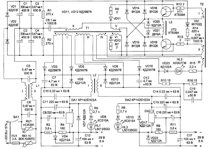
The purpose SMPS components:
SA1 - the power switch;
FU1 - the fuse that protects the power supply line in an accident in the source;
RK1 - the thermistor that limits the starting current to charge the capacitor C1.C4 to safe for diodes VD1 and VD2 value;
RU1 - varistor, shunt overvoltage pulses coming from the network;
C5-C6-L1 - the network filter that suppresses high-frequency oscillations generated by Converter;
VD1-VD2-C1, C4-R1-R2 - network rectifier with a capacitive divider.
Resistors R1 and R2 drain the capacitors C1…C4 when you turn off the source from the network. The capacitance of the capacitors C1, C3 and C2, C4 in the General case are not the same, and the midpoint of the divider offset about half of the supply voltage. However thanks to the capacitor C8 in the steady state current through the bias power transformer T1 does not flow;
C7-C10-C11-L2-VD3-VD5-VD6 and C13 C15…-L2-VD9-VD10-VD16 - output rectifiers with a smoothing LC-filters, made under the scheme Mac Estuary. Electrolytic capacitors immediately after the output of the rectifiers is invalid, as these capacitors will quickly overheat due to the high ripple voltage and will be released from system;
C9-C12-DA1-R3-R4-VD4-VD7 and C16-C17-DA2-R9-R11-VD17-VD22 - the compensation voltage (Low Drop) protecting overload and short circuit. At the time of turning off the source diodes VD4 and VD22 protect circuits DA1 and DA2 from reverse voltage with capacitors C9 and C16, and the diode VD7 and VD17 - reverse-voltage capacitors C12 and C17. Stable output voltage can be changed by selection of resistors R3, R4и R9, R11;
R5-HL1-VD8 and R8-HL2-VD13 - chain indication of tripping stabilizers;
T1 - pulse power transformer galvanically separating the input and output source power;
R6, R7, VD11, VD12-components that prevent the flow of currents through through key transistors. Until dissolve the excess carriers in the base circuit of one transistor, the other transistor cannot open;
VD14, VD15, VD18, VD19 - damping diodes;
VD20-VD21 - limiter voltage pulses EMF reactor L3;
L3 - reactor, providing the opening delay of the transistors due to the current limitation of collectors. Thanks to safe switching transistors does not occur secondary sample semiconductor structure;
VT1, VT2 - switching transistors. Voltage coming from their bases transformer T2 and from the chains that prevent the through current, should be about the same. In this case, when the polarity of the voltage from T2. is compensated for these voltages and currents databases via transistors not closed flow;
R15-HL3-VD23 - elements of light indication of activation of the SMPS;
C19-R10-R16-T1-T2 - chain of positive feedback, providing the excitation of the transducer. By increasing the consumption of power conversion frequency increases, and the voltage on all windings the transformer T1 is reduced. But to the transitions of the base-emitter of the switching transistors applied almost the same voltage as the voltage on the windings the switching transformer T2 is almost not reduced due to the reduction capacitive resistance of the capacitor C19. Thanks to the capacitor C19 transistors VT1 and VT2 are not working in the active region, which has increased manifold would dissipated in them the power and decreased the efficiency of the Converter. Direct the connection of the capacitor C19 with IV winding of the transformer T1 is unacceptable, since then key the transistors will be damaged;
C18-R14-VS1 - the trigger circuit generates a pulse after inclusion of the source, which opens the transistor VT2, causing the auto gen start.
T2 - saturated switching transformer. The parameters of the magnetic circuit and the number of turns in the windings, set the frequency of oscillation of the Converter. The smaller dimensions and fewer turns in the windings, the higher the frequency conversion.
Integrated voltage regulators DA1, DA2 type can CREA replace LT1083. Each of the chips mounted on heatsink size a cooling surface 350 cm2. The switching transistors VT1 and VT2 (CTA) are replaced by KT838A CTA, BU208A or similar with reverse voltage less than 1000 V and current collector not less than 4 A. Each of the transistors mounted on the heat sink area of 60 cm2.
A dinistor VS1 (CND) can be replaced by the DB-3, DB-4 or at any dinistor from the series. KN. Diodes VD1 and VD2 - type CDG. they can be replaced by CDD, or HFA06TB120 similar with reverse voltage more than 1000 V and direct current of not less than 8 A.
Diodes VD3, VD5, VD9, VD16 (KDV) replaced by CDA, 30CTQ100, SFA1604G or similar with reverse voltage less than 100 V, the direct current of at least 10 And and the frequency is below 100 kHz. Each diode is fixed on a heat sink area a cooling surface of at least 50 cm2. Install diodes on the heatsink mandatory. Instead diode VD4, VD6, VD7, VD10, VD17, VD20, VD22(KДl212A) you can use GDB, KDB (IN), KDB (IN), CDA, MUR120, SF34 or equivalent with a reverse voltage of at least 100 In direct current of at least 1 A. the Diodes VD11, VD12 (CDA) you can substitute any diodes of the series KD, KD, diodes KDA, 1N5822, 31DQ10, 50SQ080, or 50SQ100 similar direct current of at least 3 A. Damper diodes VD14, VD15, VD18, VD19 (BY228) replaced by KD243ZH KDE KDD, KDD, A, 1F7, 1N4007. 1N5408, 1N5399, 150EBU02, HER208, BYM26E, PART NO BYV26E, FR157, FR207, RL207 or similar with reverse voltage less than 1000 V and direct current of at least 1 A. Diode VD23 (CDA) you can replace KDA, KDA, KDA, KDA, KDA or CDB.
Instead of Zener VD8, VD13 (CSA) suitable DD, CSA (B), CSA or equivalent voltage stabilization from 14 to 20 V and a maximum current of at least 10 mA. instead VD21 (the d816a), DB or similar with voltage stabilization from 22 V to 30 V and the maximum current of at least 150 mA.
LEDs HL1 and HL2 (L5013SGD) can be replaced by L5013SGD-B, L5013UEBC-B, HL3 (ALGM) - for every led series AL, AL307.
Capacitors C1, C2, C12, C17 - type K50-27, C50-35; C3…C7, C10, C13, C14 C18, C19 - K73-16, K73-17; S8 - C-10, C-12, C-24; C9, C11, C15, C16 - KEA-II, K50-6, K50-27, C50-35. Capacitor C8 must have a capacity of not less than 550 OPTIONS and may have a capacity of from 0.47 to 1.5 UF. The capacitance of the capacitor C19 can be from 0,022 to 0,047 UF. The capacitors can be replaced by any similar designed for the same voltage.
Resistors R1, R9, R11, R15 may be the type MLT, ALT C2-22 C2-23, and R10 and R16 - C5-MV, C5-37 or sew-5. The resistors can be replaced by any similar rated at the same power. Varistor RU1 (VCR391) you can replace the JVR-10N361K, JVR-14N361K, JVR-20N361K,JVR-10N391K,JVR-14N391K,
JVR-20N391K, JVR-10N431K, JVR-14N431K, JVR-20N431K or similar, thermistor RK1 (SCK-103NTC) MZ92-P220RM, MZ92-R220RM, MZ92-P330RM, MZ92-R330RM or similar.
The Inductor L1 performed on the ring alsever TCC or TO size Chg. The windings I and II contain 20 turns of wire MGTF, PELSHO or sew-2 01 mm and are wound with two wires. Additionally one of the conclusions of each winding is recommended to wear a ring of ferrite MNM K10h6h3, use a ferrite rod magnetic antenna of the receiver as L1 is not recommended, as much will increase the stray field of the inductor, and screening high-voltage inductor it is rather problematic.
The Inductor L2 wound on the magnetic core. Sh ferrite 2000NM. The windings I and II contain 75 turns wire PETV, PEPCO or sew-2 01,7 mm each and are wound with two wires. Kern core has a non-magnetic gap of 0.3…0.5 mm from the PCB or Micarta. To reduce stray fields choke shield, wrapping outside all three rod one revolution brass band of thickness of 0.05 to 0.1 mm....the ends of the tape soldered to each other.
The Reactor L3 ferrite ring MNM or "Micrometals" CHH. Each of Polubotok has a coil of wire. MGTF PETV, sew-2 or conventional bonding wire 0.6 mm.
The Transformer T1 performed on three stacked ferrite rings ferrite MNM, MNM-A or MNM-17 size Chg. The windings I and III each contain 15+15 turns wire 01,7 mm; winding II - 264 revolution 0.9 mm; winding IV - 7 turns of 0.41 mm; winding V and VI - 1 coil Wire of 0.25 mm. - MGTF, PELSHO or sew-2. Winding II is wound first and contains 4 layers insulation: after each winding 66 of turns is laid a layer of PTFE or Mylar film.
The Transformer T2 ferrite ring MNM-AND CHS. All windings (I, II and (III) contain 8 turns of wire. MGTF, PELSHO or bonding wire in a reliable the insulation. In the windings I and II wire 0.3 mm, and in III - 0,42 mm.
Design. The mutual arrangement of conductors and parts source is not critical. My source is mounted Assembly. The diameter of the wires that connect the parts operating under high voltage should be 1 mm and more wires connecting the source to the load is not less than 1.7 mm. All wires must be reliable in isolation.
The establishment of. Attention! Part of the source elements is high voltage dangerous to life. Follow the rules safety!
Before switching on the power source should carefully check the installation for compliance the scheme SMPS collected from the healthy parts, usually begins to work immediately. If the UPS is turned on, the auto generation does not occur (HL3 led is not lit), then you need to change shift (swap ends) or IV winding of the transformer T1, or winding III of transformer T2.
If mains voltage 220 V idling current source 40 mA more (measured after network filter), shall be increased the number of turns of all the windings of the transformer T1. If the output voltages are different from 29 In, they can to set the selection of the resistances R3 and R11.
Author: E. Mokotow, Taganrog, Rostov region