


")

In Amateur practice, as well as, repair of equipment, can handy portable high voltage power source, battery powered. Such a device may be useful when checking the reverse voltage of the diode, voltage of the high voltage stabilizing Zener voltage ignition neon lights, as well as for testing of high-voltage transistors.
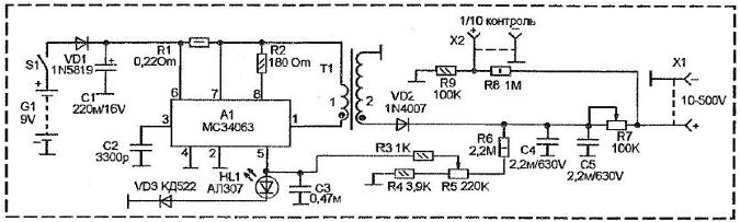
The following is a description portable high-voltage source, constant the output voltage of which can be adjusted continuously from 10 to 500 V. the Output the current depends on the voltage (the higher the voltage the lower the current). When the maximum voltage the current is 1.5 mA. Powered generator from "the Crown" (a galvanic battery with a 9 V) having no connection with the mains. And yet, working with him to observe safety precautions (not to kill kill, but to shake the can).
The primary power source battery G1. Voltage 9 V across the diode VD1 (used for protection from accidental wrong connection of power) is supplied to the DC-DC Converter transformer output on the chip type A1 MS. This the chip is designed for circuits DC-DC converters low power or more power, but with an additional key high-power transistor. Here the low-power source, because you are using your own output key of the chip.
The operation of the chip type MS was repeatedly and in detail described in various literature. Let me remind you that this pulse generator with changing latitude, which can be adjusted by means of a pin 5. This pin is used for the circuit stabilize the output end (secondary) voltage.
The resistor R1 operates in the circuit protection of the output circuits from overcurrent. When the voltage across R1 exceeds the reference value, the output stage is disabled.
The conversion frequency is set by the capacitance of the capacitor C2, which works in castorocauda generator circuit.
Loaded chip. A1 the primary winding of the boosting high frequency pulse transformer T1. The AC voltage from the secondary winding of is supplied to the rectifier diode VD2.
To maintain the DC output voltage is stable and adjust output voltage circuit is used R6-R5-R4. Here we use internal the stabilization scheme/of the output voltage present at A1. Its essence that chip changes the latitude of the output pulses so that the voltage at its pin 5 was equal to 1.25 V. that is, if the voltage at pin 5 is less than 1.25 In the latitude of the output pulses supplied to the primary winding of the transformer T1 will increase, and if the voltage at pin 5 is greater than 1.25 - lat will be to diminish.
Thus, the PWM scheme will work so that at pin 5 to maintain a 1.25 V. Now we need to make the voltage at pin 5 dependent on the output voltage of the transformer (secondary winding). The purpose R4-R5-R6 representing an adjustable voltage divider, is used to apply this ratio dependence of the output voltage from the voltage vyv. 5.
Led HL1 burning should not, in its place it could be put stabistor 1.8…2 V, but the led easier to acquire. In this scheme, he performs the functions of stabistor limiting the maximum voltage at pin 5 A1. The need in such a limiter occurred after was spoiled one instance chip MS during the rapid rotation of the handle of the resistor R5. The problem that the adjustment range of the output voltage here is very wide, and when quick adjustment of the voltage on the capacitors C4 and C5 do not have time to change accordingly. This is especially noticeable at idle or high impedance load. As a result, at some point in time the voltage on pin 5 A1 may be too high and damage the input of this comparator of the chip. To prevent this from happening and have the chain VD3-HL1-C3-R3. Practically, this parametric stabilizer does not allow increasing the voltage at pin 5 A1 above 2.5 V. furthermore, when a sharp adjustment on the decline the output voltage of this circuit generates an additional current discharging capacitors C4 and C5 (at some point quick adjust maybe even flashing led).
Variable resistor R7 serves to increase the output resistance of the source. This may be required when checking diodes reverse breakdown. You connect to terminals X1 diode in the reverse direction, to the terminals x2 connect multimeter (which will show a 10 times lower voltage than the diode) and begin gradually increase the voltage. As soon as the breakdown voltage, which shows multimeter stops growing or falling, despite adjustment to increase the resistor R5. Thus, R7 is resistance to limit the current in the test circuit. Size restrictions can be set by adjusting R7, and if it doesn't have to turn it the knob to the minimum position.
The transformer T1 is wound on a ferrite ring external diameter of 28 mm. The ferrite ring is necessary before winding process, is sandpaper to give it the edges of the caps, and then cover the ring with a thin layer of epoxy varnish. After drying Pak check ring surface in the absence of burrs and sharp edges (for example, due to defects in hardening of the lacquer). All burrs and edges need smooth and, if necessary, again varnished.
After the final curing of the lacquer secondary spool the winding. It contains 2000 turns of wire sew 0,12 wound uniformly in bulk in the ring, but so as to leave a small gap between the beginning and the end of winding. Winding is necessary to do so. to areas with a large difference in the number of turns is not touch each other. That is, to wind in bulk, but uniformly moving in one direction, and not back and forth. After winding the secondary winding of the need to cover it with a layer of varnished cloth or fluoropolymer film and on this surface to wind the primary winding - 15 of turns of wire sew 0,61 (or other diameter from 0.5 to 1 mm). Winding distribute evenly over the surface of the secondary winding. Both winding wind in one and the same direction. The diagram shows how they need to be stateroute.
Author: V. We Can Say