


")

The proposed power supply, designed in a wide range to smoothly change the output voltage (Fig. 6.11). Its peculiarity lies in the use of adjustable negative feedback from the output of the unit at cascade transistor VT1, connected in parallel to the output of the diode bridge. This cascade is parallel regulatory element and is controlled by the signal from the output of the single stage amplifier to VT2. The output signal VT2 depends on difference between voltages applied to the variable resistor R7, included in parallel to the output of the power supply, and voltage reference diodes VD3, VD4.
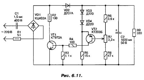
Essentially, the circuit is an adjustable parallel stabilizer. The role of the ballast resistor plays a quenching capacitor C1, the role of parallel the controlled element is a transistor VT1. Running this power supply as . When turning on the transistors VT1 and VT2 are locked through the diode VD2 occurs the charge storage capacitor C2.
When reaching to the base of transistor VT2 voltage equal to the reference diodes VD3, VD4, transistors VT2, VT1 begin to deny it. Transistor VT1 bypasses the output of the diode bridge, and the output voltage begins to fall, which reduces the voltage on the cumulative the capacitor C2 and to the locking of the transistors VT2 and VT1. This, in turn, causes a reduction in shunting the output of the diode bridge, increasing the voltage on C2 and unlocking VT2, VT1, etc.
Due to the current thus negative feedback output the voltage remains constant (stable) when the load R9 and without it, at idle. Its value depends on the position of the engine potentiometer R7 Top (the scheme) the position of the slider corresponds to a larger output voltage.
Maximum power output of those devices is equal to 2 watts.
The limits of adjustment of the output voltage from 16 to 26 In, and when shorted the diode VD4 limits range from 15 to 19.5 V. In these ranges when disabling R9 (load dump) the increase of the output voltage does not exceed of one percent. VT1 is running in AC mode: when working on the load R9 - linear mode; idle - mode pulse width modulation (PWM) with the frequency of the ripple voltage on the capacitor C2 is 100 Hz. The pulses the voltage at the collector of transistor VT1 have flat fronts. Linear mode is a lightweight, transistor VT1 is heated a little and can work almost without a radiator.
Little heat is in the lower position of the slider of the potentiometer R7 when the minimum output voltage. At idle, disabled load R9, the thermal regime of the transistor VT1 is deteriorating in the upper position of the engine R7 In this if the transistor VT1 must be installed on a small radiator, for example, in an aluminum plate of square shape with sides 3 cm, thickness 1…2 mm.
The control transistor VT1 - average power, with a large transmission coefficient (composite). Its collector current should be 2-3 times greater than the maximum load current. The collector voltage VT1 must not be less than the maximum output the voltage of the power supply. As VT1 can be used n-p-n transistors CTA, CTA, CTA etc Transistor VT2 works in the regime of low currents, so we're all on the low-power p-n-p transistor - CTA…, CTA…G, QTA/B, CTA/B.
According to the principle of this scheme can be constructed similar power supplies on other required capacity values.
Author: A. P. Seman