


")

The voltage, V +/-32
Nominal (maximum) power output at 4 Ohms, watts 45(65)
Harmonic distortion, % in the frequency range:
20…5000 0,003
5000 20000…0,01
Nominal input voltage, mV 0,775
Nominal frequency range, 20 Hz 100000…
Frequency response in the frequency range, dB 0,25
The signal-to-noise ratio (dB) 100
The slew rate of the output signal, V/μs 60
Amplifier circuit:
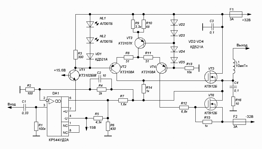
Particularly the scheme will not describe, except to say that the stabilization of the output stage is carried out at the expense of the transistor VT3, which is mounted on one heat sink with VT5. HL1 and HL2 indicate overloading of the amplifier and at the same time reduce, this occurs when signal distortion.
The output transistors are mounted on the radiator area 400 sq cm Coil L1 dangle on the frame outside diameter of 20 mm and contains 28 turns of wire sew-2 to 1.0. Transistors CT can be replaced by CTA or CTB.
The establishment comes down to setting the quiescent current of the output transistors within a 200-300mA…the selection of resistors R7 and R10.
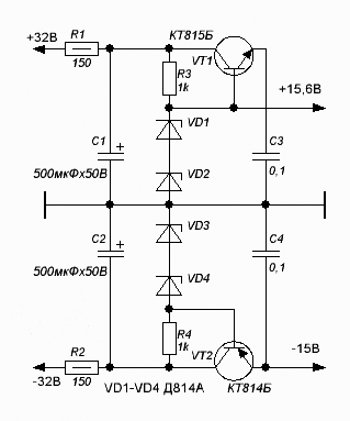
The power source for pre-amplifier stage can be collected as follows:
The printed circuit Board here [attachment=7]