


")

In order to change the ringtone played UMS, you need it sound or within a few tenths of a second after the end of the file pulse high logic level to the input "Select ringtone" (VM) chip synth. In the latter case, the next tune begins to play regardless of the logic level at the input "start" (S)
In Fig. 1 shows the scheme of a simple call that automatically goes through all available in memory UMS ringtones.
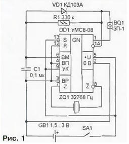
On pin 13 of the chip DD1 constantly applied logical 1, so after the power starts reproduction of the first from ringtones. Short pulses of low level at the inverted output DD1 (pin 14) through the diode VD1 drain the capacitor C1. Although the intervals between pulses this the capacitor is charged through a little resistor R1, while playing melody the voltage across it does not reach the threshold of the entrance of the VM. It will only happen after the end of the melody and the termination of the pulse, when the output 14 DD1 will install a DC voltage close to the supply. In the result will start playback of the next song, and again appeared at pin 14 DD1 pulses discharges the capacitor C1.
To the time constant circuit R1C1 meet conflicting demands. One hand, it should be high enough so that the capacitor does not have time be charged on the intervals between pulses, on the other - at the end of the melody he must have time to recharge before it will repeat. The situation is complicated by the fact. found ringtones, consisting of two or more parts, separated by a fairly long pause. This melody can be replaced before the sound completely.
Call collect surface mounting directly on the pins of the chip DD1. in which is better to apply US-08 or US-08. Also suitable WMS-01. Diode VD1-any low-power silicon, for example, series CD. CD. KD521. KD522. Resistor R1 - MLT-0.125. capacitor C1 - km-6. Establishing is the selection of the resistor R1. If the tune gives way too early you should increase the resistance. If it "loops", the resistance should be reduced.
Embedding the call in hours, which has its own generator operating at a frequency of 32768 Hz. quartz resonator ZQ1 can be eliminated. Pin 3 of chip DD1 in this the case is connected to the pin 5. and on pin 7 signal generator. Can connecting pin 7 directly with one of the findings of the quartz resonator hours, which is determined experimentally.
More complex call, the diagram of which is shown in Fig. 2, guaranteed plays back all recorded in the memory of the synthesizer melodies completely. In addition to UMC DD4. it offers the nodes of the formation of the control pulses (DDI.2, DD2, DD3.3, DD1.6). output disable (DD3.1, DD3.2, DD3.4) and the oscillator (DD1.1, DD1.3-DD1.5).
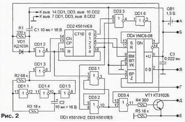
After applying power to direct the output of the chip DD4 (pin 1) set to low level and the capacitor C1 is charged through the resistor R1 As only the voltage on the capacitor drops below the switching threshold of the element DD1.2. a logic low at the output of the latter will be replaced high. It translate DD2 counter to its original state and set the trigger of the logical elements DD3.1 and DD3.2 in a condition prohibiting the passage through the element DD3.4 the signal from the output 14 of the chip DD4 to the base of transistor VT1 In the initial state counter DD2 high logic level of its output (pin 3) through the elements DD3.3 and DD1.6 is supplied to pin 13 of the chip and DD4 starts generating ringtones. But the first high level pulse at pin 1 of the EMC through the diode VD1 drain the capacitor C1. and low logic level at the exit of the element DD1.2 will allow the counter DD2.
With each pulse of the clock generator (elements DD1.1. DD1.4, DDI.5) the outputs of the counter pulses appear alternately high level. It outputs 1 and 2 are connected respectively to the inputs of the "Select ringtone" (VM) and Stop (R) chip DD4, so after the first clock pulse generator melody will change, but it will not sound as output signals do not pass DD4 through the element DD3.4. The second pulse synthesizer is stopped.
The third pulse generator will establish a high logic level at pin 7 counter DD2. Elements DD3.3 and DD1.6 sends it to pin 13 of the chip and DD4 starts playing the next tune. At the same time will switch the trigger DD3.1. DD3.2. allowing the passage of a sound signal through the element DD3.4. The next clock pulse will set the high logic level at pin 10 counter DD2, who will arrive at its output 13, and prohibit the further expense. After the end of the tune capacitor C1 is charged again and the described cycle is repeated.
Details of the call can be mounted on the Board, sketch traces and the layout of which is shown in Fig. 3.

Chip to DD4 should establish a panel that will allow, if necessary to quickly change a set of tunes. Except as indicated on the diagram UMS-08, DD4 suitable WMS-01. Chip UMS-03 and US-05 in this case the so how to stop playing the melody shortly after the removal of the enabling signal at pin 13. Chips instead of KIA you can install CIA, taking into account the differences in the appointment of their findings. Transistor VT1 can be any of the series CT, KT315 or CTS. Diode VD1 - any low-power silicon. Resistors MLT-0,125. Capacitors C1 and C2 (oxide) - K50-35 or K50-40, C3 - km-5. Km-6.
The power source voltage of 3 To connect to the pads B (plus) and (minus). Galvanic element GB1 size A (AAA) in this case is not need. It is installed, if the device works in conjunction with e clock, powered by a voltage of 1.5 V from a single galvanic cell. With positive pole last connect the contact area And, with negative V. and the alarm switch must break one of these chains. In sum, the two elements will give the necessary 3 V.
The pad G is connected to the output of the crystal oscillator clock. If necessary (for example, if the oscillator frequency in hours different from 32768 Hz) can to enable the resonator to the desired frequency between pins 7 and 8 of the chip DD4. as it was shown in Fig. 1. In this case, its pin 3 should be connected to a power source and to a common wire (pin 2).
The output signal of the call is removed from the emitter (contact area (E) or manifold (pad E) of the transistor VT1. In the first case it the collector is connected to the power source (platform B) directly, in the second - through a resistor or other load.
In Fig. 4 shows how to connect the call to a common Electromechanical hours M. Removing them from the cover, gently otpaivaete from a printed circuit Board containing all the electronic parts of the watch, the terminals of the coil L1. extract from her body, and then charge. In the places marked in the figure by crosses, printed wires cut. Pads, battery and switch alarm SA1 connect a jumper wire from the insulated wire.
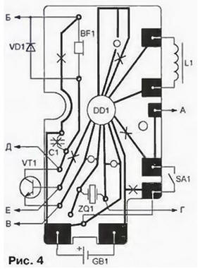
Available in hours the transistor VT1, which can be substituted by domestic series CT, together with VT1 call form a composite transistor, managing the sound emitter BF1. The 3 V supply will go at this stage pad B. in Parallel with the emitter, connect the diode VD1 - any of series CD, CD, KD521, KD522. Available in some instances hours capacitor C1 is a capacitance of 1000 pF are removed. Board hours and call connect six wires. Then install charge hours to the place and restore it the connection to the coil L1.
Correctly assembled the call does not require networking. When testing is necessary note that a beep will appear after 5…7 after voltage power. The duration of the pause between the tones can be adjusted by selection of the resistor R1.
Author: A. Shitov, Ivanovo