


")

Very often, the hardware fails at the time of its inclusion in the network. Happens this is because pulse surge current in the power supply with a powerful network transformer and smoothing capacitors a large-capacity. Inherent this phenomenon and pulsed power supplies.
The usual method of reducing the inrush current is the installation of a powerful low-impedance resistors on the input of the power supply, which then are bridged by relay contacts. But this scheme protects with bad periodic power outage, because it has a slow the momentary.
The proposed device (Fig.1) provides reliable protection of equipment and can be included at the input of any power source. It is fed by AC current (one phase in a three phase inclusion of the protected device). Rectifier VD1 is connected through the ballast capacitor C1, the capacitance of which limits current draws. Resistor R2 discharges the capacitor C1 after disconnection of the mains voltage, and the resistor R1 limits the initial current of C1 (at the moment of inclusion).
If you want to nourish device from another voltage, it is necessary to convert the capacitance C1.

Zener diode VD2 limits the voltage at 15 V. the Chain of R5-C4-VD4 is to install the RS-flip-flop on the elements DD1.2, DD1.3 in initial status when power (diode VD4 quickly discharges C4 by the network failure). At the moment of switching of audio input devices 8 DD1.2 - low level.
For logical element 2I-NOT the level - switching. Feature of RS-flip-flop is that it works from the first zero pulse, and the rest not reacts.
Integrated circuit R3-C3-VD3 creates a temporary delay (about 3 C). The charge of the capacitor C3 is coming from rectifier VD1 through resistor R3 (diode VD3 quickly discharges C3 in case of loss of mains voltage). At the starting point on input 8 DD1.2 - low level, and at the entrance DD1 13.3 - high. With this the state of the input signals of the RS-flip-flop at the output 11 DD1.3 - low level, and transistor VT1 is closed. DA1 chip is de-energized, triac VS1 is switched off, and in series with the load RL connected current-limiting the resistor R10. After charging of the capacitor C4 at pin 8 DD1.2 is a high level. Single signals on both inputs of RS-trigger match the mode of information storage.
3 with the inlet 13 DD1.3 "0" appears, the trigger turns over and takes the a high level on the transistor VT1. The transistor opens and turns on the led chip DA1. Chip consists of an infrared emitting diode, optically connected with the detector bilateral voltage transition through zero and triac-output scheme. The output circuit DA1 opens triac VS1 (pulse the output current of the chip can reach 1, but this output is not loaded constant load).
The thyristor VS1 open, bypasses the limiting resistor R10, and full voltage supplied to the load.
In case of loss network, the capacitor C4 discharges through VD4, input 8 DD1.2 is formed low level, and the trigger returns to its initial state, i.e. transistor VT1 is served low level.
The transistor is closed, disables the triac VS1, and in the load circuit is switched on the limiting resistor R10. When the advent of the Internet and the expiration time of exposure (3) a trigger is switched, and joined triac bypasses the limiting resistor.
Time delay can be adjusted by changing the values of the chain R3-C3.
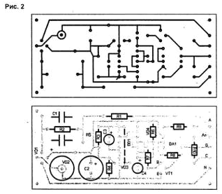
The device is made on the PCB size 91x41 mm (Fig.2).
The resistance of the resistor R10 is selected based on the maximum allowable current of the protected device.
Triac VS1 choose largest the necessary operating current. Note that the currents switched triacs, are temperature dependent.
Therefore, the triac must be installed on the radiators. One the circuit output can DA1 connect only one triac.
When checking the device mains voltage was varied in the range from 120 to 270 V. If such a wide the range is not needed, the capacitance of the capacitor C1 can be reduced by half.
Author: V. Kalashnik, Voronezh